OneNAND512Mb(KFG1216U2B-xIB6)
3.13 ECC Operation
FLASH MEMORY
The OneNAND device has on-chip ECC with the capability of detecting 2 bit errors and correcting 1-bit errors in the NAND Flash
Array memory main and spare areas.
As the device transfers data from a BufferRAM to the NAND Flash Array memory Page Buffer for Program Operation, the device ini-
tiates a background operation which generates an Error Correction Code (ECC) of 24bits for each sector main area data and 10bits
for 2nd and 3rd word data of each sector spare area.
During a Load operation from the NAND Flash Array memory Page, the on-chip ECC engine generates a new ECC. The 'Load ECC
result' is compared to the originally 'Program ECC' thus detecting the number and position of errors. Single-bit error is corrected.
ECC is updated by the device automatically. After a Load Operation, the Host can determine whether there was error by reading the
'ECC Status Register' (refer to section 2.8.26).
Error types are divided into 'no error', '1bit correctable error', and '2bit error uncorrectable error'.
OneNAND supports 2bit EDC even though 2bit error seldom or never occurs. Hence, it is not recommended for Host to read 'ECC
Status Register' for checking ECC error because the built-in Error Correction Logic of OneNAND automatically corrects ECC error.
When the device reads the NAND Flash Array memory main and spare area data with an ECC operation, the device doesn't place
the newly generated ECC for main and spare area into the buffer. Instead it places the ECC which was generated and written during
the program operation into the buffer.
An ECC operation is also done during the Boot Loading operation.
3.13.1 ECC Bypass Operation
In an ECC bypass operation, the device does not generate ECC as a background operation. The result does not indicate error posi-
tion (refer to the ECC Result Table).
In a Program Operation the ECC code to NAND Flash Array memory spare area is not updated.
During a Load operation, the on-chip ECC engine does not generate a new ECC internally. Also the ECC Status & Result to Regis-
ters are invalid. The error is not corrected and detected by itself, so that ECC bypass operation is not recommended for host.
ECC bypass operation is set by the 9bit of System Configuration 1 Register (see section 2.8.19)
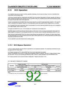
ECC Code and ECC Result by ECC Operation
Program operation
Load operation
Operation
ECC Code Update to NAND ECC Code at BufferRAM Spare ECC Status & Result Update
1bit Error
Flash Array Spare Area
Update
Area
to Registers
Update
Pre-written ECC code(1) loaded
Pre-written code(1) loaded
ECC operation
ECC bypass
Correct
Not update
Invalid
Not correct
NOTE:
1. Pre-written ECC code : ECC code which is previously written to NAND Flash Spare Area in program operation.
92

 SAMSUNG [ SAMSUNG ]