OneNAND512Mb(KFG1216U2B-xIB6)
FLASH MEMORY
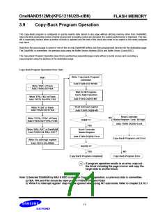
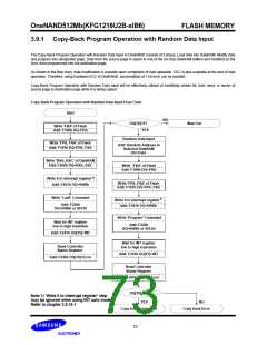
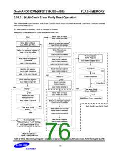
The Copy-Back steps shown in the flow chart are:
•
•
•
Data is read from the NAND Array using Flash Block Address (FBA), Flash Page Address (FPA) and
Flash Sector Address (FSA). FBA, FPA, and FSA identify the source address to read data from NAND Flash array.
The BufferRAM Sector Count (BSC) and BufferRAM Sector Address (BSA) identifies how many sectors
and the location of the sectors in DataRAM that are used.
The destination address in the NAND Array is written using the Flash Copy-Back Block Address (FCBA),
Flash Copy-Back Page Address (FCPA), and Flash Copy-Back Sector Address (FCSA).
•
•
The Copy-Back Program command is issued to start programming.
Upon completion of copy-back programming to the destination page address, the Host checks the status
to see if the operation was successfully completed. If there was an error, map out the block including the
page in error and copy the target data to another block.
72

 SAMSUNG [ SAMSUNG ]