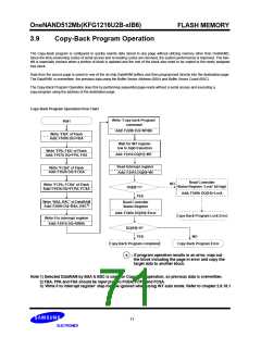
OneNAND512Mb(KFG1216U2B-xIB6)
FLASH MEMORY
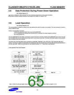
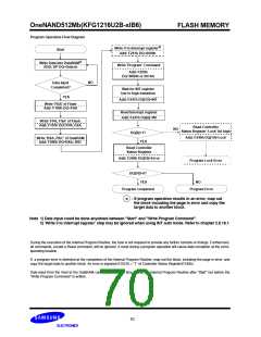
3.8
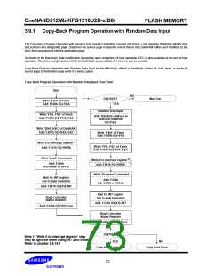
Program Operation
See Timing Diagram 6.11
The Program operation is used to program data from the on-chip BufferRAMs into the NAND FLASH memory array.
The device has two 2KB data buffers, each 1 Page (2KB + 64B) in size. Each page has 4 sectors of 512B each main area and 16B
spare area. The device can be programmed in units of 1~4 sectors.
The architecture of the DataRAMs permits a simultaneous data-write operation from the Host to one of data buffers and a program
operation from the other data buffer to the NAND Flash Array memory. Refer to Section 3.93.9.2, "Write While Program Operation",
for more information.
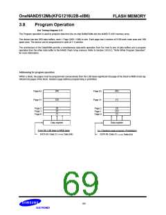
Addressing for program operation
Within a block, the pages must be programmed consecutively from the LSB (least significant bit) page of the block to MSB (most sig-
nificant bit) pages of the block. Random page address programming is prohibited.
(64)
(64)
Page 63
Page 31
Page 63
Page 31
:
:
(1)
:
(32)
:
(3)
(2)
(1)
Page 2
Page 1
Page 0
(3)
(32)
(2)
Page 2
Page 1
Page 0
Data register
Data register
From the LSB page to MSB page
DATA IN: Data (1)
Ex.) Random page program (Prohibition)
DATA IN: Data (1)
Data (64)
Data (64)
69

 SAMSUNG [ SAMSUNG ]