OneNAND512Mb(KFG1216U2B-xIB6)
FLASH MEMORY
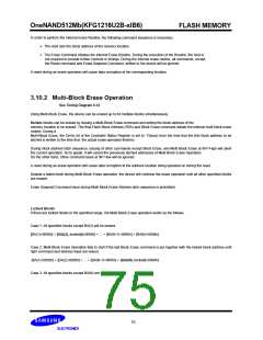
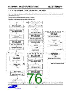
3.10.3 Multi-Block Erase Verify Read Operation
After a Multi-Block Erase Operation, verify Erase Operation result of each block with Multi-Block Erase Verify Command combined
with address of each block.
If a failed address is identified, it must be managed by firmware.
Multi Block Erase/ Multi Block Erase Verify Read Flow Chart
Write ’FBA’ of Flash
Add: F100h DQ=FBA
Start
Write 0 to interrupt register1)
Add: F241h DQ=0000h
Write ’FBA’ of Flash
Add: F100h DQ=FBA
Write ’Block Erase
Command’
Write 0 to interrupt register1)
Add: F241h DQ=0000h
Add: F220h DQ=0094h
Read Controller
Status Register
Write ’Multi Block Erase’
Command
Wait for INT register
low to high transition
Add: F240h DQ[10]=Error
Add: F220h DQ=0095h
Add: F241h DQ=[15]=INT
DQ[10]=0?
Read Interrupt register
Add: F241h DQ[5]=EI
Wait for INT register
low to high transition
NO
YES
Add: F241h DQ=[15]=INT
NO
Erase completed
DQ[5]=1?
YES
Read Interrupt register
Add: F241h DQ[5]=EI
Read Controller
Status Register
Erase Error
Add: F240h DQ[10]=0
NO
NO
DQ[5]=1?
YES
Final Multi Block
Erase Address?
Write ’FBA’ of Flash
Add: F100h DQ=FBA
YES
Read Controller
Status Register
Multi Block Erase completed
Write 0 to interrupt register1)
Add: F241h DQ=0000h
Add: F240h DQ[10]=0
Multi Block Erase Verify Read
NO
Final Multi Block
Erase?
Write ’Multi Block Erase
Verify Read Command’
YES
Add: F220h DQ=0071h
Wait for INT register
low to high transition
Read Controller
Status Register ‘Lock’ bit high
Add: F241h DQ=[15]=INT
Add: F240h DQ[14]=Lock
Multi Block Erase /
Block Erase Lock Error
Note 1) ’Write 0 to interrupt register’ step may be ignored when using INT auto mode. Refer to chapter 2.8.18.1
76

 SAMSUNG [ SAMSUNG ]