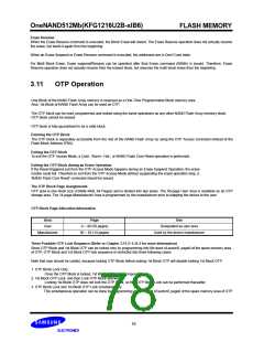
OneNAND512Mb(KFG1216U2B-xIB6)
3.10 Erase Operation
FLASH MEMORY
There are multiple methods for erasing data in the device including Block Erase and Multi-Block Erase.
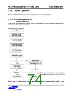
3.10.1 Block Erase Operation
See Timing Diagram 6.126.12
The Block Erase Operation is done on a block basis. To erase a block is to write all 1's into the desired memory block by executing
the Internal Erase Routine. All previous data is lost.
Block Erase Operation Flow Chart
Start
Write ’FBA’ of Flash
Add: F100h DQ=FBA
Write 0 to interrupt register1)
Add: F241h DQ=0000h
Write ’Erase’ Command
Add: F220h DQ=0094h
Wait for INT register
low to high transition
Add: F241h DQ=[15]=INT
Read Interrupt register
Add: F241h DQ[5]=EI
NO
Read Controller
Status Register ‘Lock’ bit high
DQ[5]=1?
YES
Add: F240h DQ[14]=Lock
Read Controller
Status Register
Add: F240h DQ[10]=Error
Erase Lock Error
DQ[10]=0?
: If erase operation results in an error, map out
the failing block and replace it with another block.
*
YES
NO
Erase completed
Erase Error
Note 1) ’Write 0 to interrupt register’ step may be ignored when using INT auto mode. Refer to chapter 2.8.18.1
74

 SAMSUNG [ SAMSUNG ]