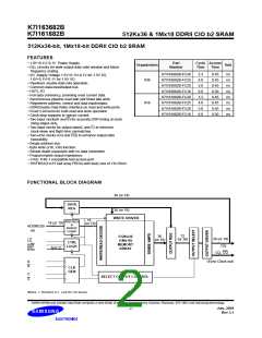
K7I163682B
K7I161882B
512Kx36 & 1Mx18 DDRII CIO b2 SRAM
GENERAL DESCRIPTION
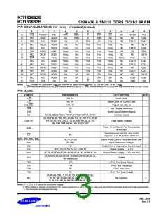
The K7I163682B and K7I1161882B are 18,874,368-bits DDR Common I/O
Synchronous Pipelined Burst SRAMs.
They are organized as 524,288 words by 36bits for K7I163682B and 1,048,576 words by 18 bits for K7I161882B for K7I160882B.
Address, data inputs, and all control signals are synchronized to the input clock ( K or K ).
Normally data outputs are synchronized to output clocks ( C and C ), but when C and C are tied high,
the data outputs are synchronized to the input clocks ( K and K ).
Read data are referenced to echo clock ( CQ or CQ ) outputs.
Read address and write address are registered on rising edges of the input K clocks.
Common address bus is used to access address both for read and write operations.
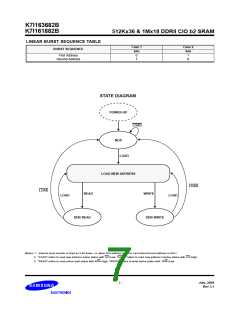
The internal burst counter is fiexd to 2-bit sequential for both read and write operations.
Synchronous pipeline read and late write enable high speed operations.
Simple depth expansion is accomplished by using LD for port selection.
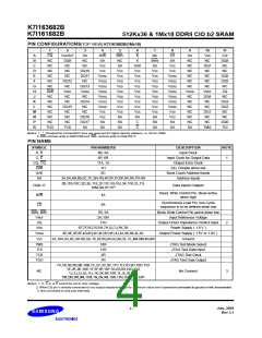
Byte write operation is supported with BW0 and BW1 ( BW2 and BW3) pins for x18 ( x36 ) device.
IEEE 1149.1 serial boundary scan (JTAG) simplifies monitoriing package pads attachment status with system.
The K7I163682B and K7I161882B are implemented with SAMSUNG's high performance 6T CMOS technology
and is available in 165pin FBGA packages. Multiple power and ground pins minimize ground bounce.
Read Operations
Read cycles are initiated by initiating R/W as high at the rising edge of the positive input clock K.
Address is presented and stored in the read address register synchronized with K clock.
For 2-bit burst DDR operation, it will access two 36-bit or 18-bit data words with each read command.
The first pipelined data is transfered out of the device triggered by C clock following next K clock rising edge.
Next burst data is triggered by the rising edge of following C clock rising edge.
Continuous read operations are initated with K clock rising edge.
And pipelined data are transferred out of device on every rising edge of both C and C clocks.
In case C and C tied to high, output data are triggered by K and K insted of C and C.
When the LD is disabled after a read operation, the K7I163682B and K7I161882B will first complete
burst read operation before entering into deselect mode at the next K clock rising edge.
Then output drivers disabled automatically to high impedance state.
Echo clock operation
To assure the output tracibility, the SRAM provides the output Echo clock, pair of compliment clock CQ and CQ,
which are synchronized with internal data output.
Echo clocks run free during normal operation.
The Echo clock is triggered by internal output clock signal, and transfered to external through same structures
as output driver.
Power-Up/Power-Down Supply Voltage Sequencing
The following power-up supply voltage application is recommended: VSS, VDD, VDDQ, VREF, then VIN. VDD and VDDQ can be applied
simultaneously, as long as VDDQ does not exceed VDD by more than 0.5V during power-up. The following power-down supply voltage
removal sequence is recommended: VIN, VREF, VDDQ, VDD, VSS. VDD and VDDQ can be removed simultaneously, as long as VDDQ
does not exceed VDD by more than 0.5V during power-down.
July. 2004
Rev 3.1
- 5 -

 SAMSUNG [ SAMSUNG ]