Preliminary
K5A3x80YT(B)C
MCP MEMORY
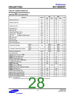
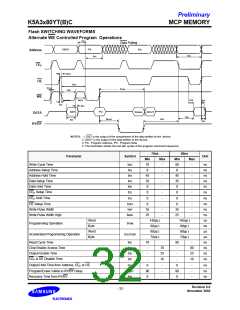
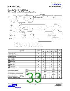
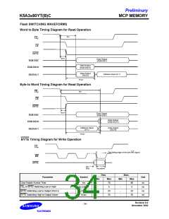
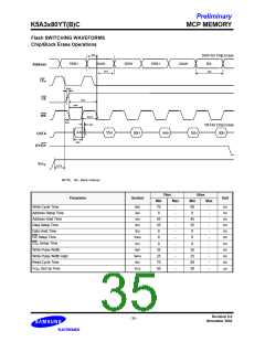
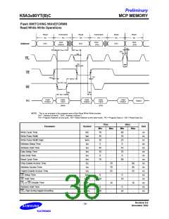
Flash SWITCHING WAVEFORMS
Alternate WE Controlled Program Operations
tAS
Data Polling
555H
PA
PA
Address
tRC
tAH
CE
F
tOES
OE
tWC
tCH
tPGM
tWP
WE
tWPH
tDH
tOE
tDF
tCS
A0H
PD
Status
DOUT
DATA
RY/BY
tCE
tBUSY
tRB
tDS
tOH
NOTES: 1. DQ7 is the output of the complement of the data written to the device.
2. DOUT is the output of the data written to the device.
3. PA : Program Address, PD : Program Data
4. The illustration shows the last two cycles of the program command sequence.
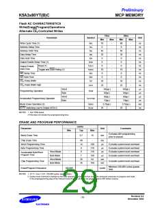
70ns
80ns
Parameter
Symbol
Unit
Min
70
0
Max
Min
80
0
Max
Write Cycle Time
Address Setup Time
Address Hold Time
Data Setup Time
Data Hold Time
tWC
tAS
tAH
tDS
tDH
tCS
-
-
-
-
-
-
-
-
-
-
-
-
ns
ns
ns
ns
ns
ns
45
35
0
45
35
0
CE Setup Time
0
0
F
CE Hold Time
tCH
tOES
tWP
0
0
-
-
-
-
0
0
-
-
-
-
ns
ns
ns
ns
us
us
ms
ms
ns
ns
ns
ns
F
OE Setup Time
Write Pulse Width
35
25
35
25
Write Pulse Width High
tWPH
Word
Byte
Word
Byte
14(typ.)
14(typ.)
9(typ.)
9(typ.)
7(typ.)
Programming Operation
tPGM
9(typ.)
9(typ.)
7(typ.)
Accelerated Programming Operation
tACCPGM
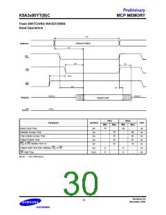
Read Cycle Time
tRC
tCE
tOE
tDF
70
-
-
80
-
-
Chip Enable Access Time
Output Enable Time
70
25
16
80
25
16
-
-
CE & OE Disable Time
-
-
F
Output Hold Time from Address, CE or OE
tOH
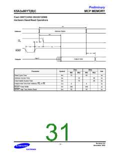
tBUSY
tRB
0
90
0
-
-
-
0
90
0
-
-
-
ns
ns
ns
F
Program/Erase Valide to RY/BY Delay
Recovery Time from RY/BY
Revision 0.0
November 2002
- 32 -

 SAMSUNG [ SAMSUNG ]