Preliminary
K5A3x80YT(B)C
MCP MEMORY
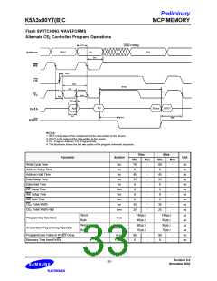
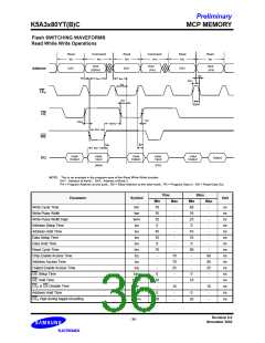
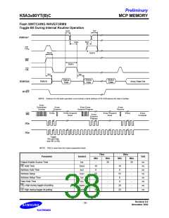
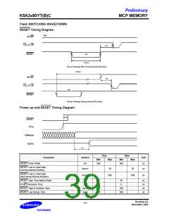
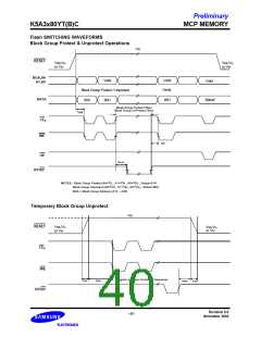
Flash SWITCHING WAVEFORMS
Read While Write Operations
Read
tRC
Command
tWC
Read
tRC
Command
tWC
Read
tRC
Read
tRC
DA2
(555H)
DA2
(PA)
DA2
(PA)
Address
DA1
DA1
DA1
tAS
tAS
tAH
tAA
tCE
tAHT
CE
F
tOE
tCEPH
OE
tDF
tOES
tOEH2
tWP
WE
DQ
t
DF
tDH
tDS
Valid
Output
Valid
Input
Valid
Output
Valid
Input
Valid
Output
Status
(A0H)
(PD)
NOTE: This is an example in the program-case of the Read While Write function.
DA1 : Address of Bank1, DA2 : Address of Bank 2
PA = Program Address at one bank , RA = Read Address at the other bank, PD = Program Data In , RD = Read Data Out
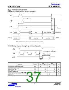
70ns
80ns
Parameter
Symbol
Unit
Min
70
35
25
0
Max
Min
80
35
25
0
Max
Write Cycle Time
Write Pulse Width
Write Pulse Width High
Address Setup Time
Address Hold Time
Data Setup Time
Data Hold Time
tWC
tWP
tWPH
tAS
-
-
-
-
ns
ns
ns
ns
ns
ns
ns
ns
ns
ns
ns
ns
ns
ns
ns
ns
-
-
-
-
tAH
45
35
0
-
45
35
0
-
tDS
-
-
tDH
-
-
Read Cycle Time
tRC
70
-
-
80
-
-
Chip Enable Access Time
Address Access Time
Output Enable Access Time
OE Setup Time
tCE
70
70
25
-
80
80
25
-
tAA
-
-
tOE
-
-
tOES
tOEH2
tDF
0
0
OE Hold Time
10
-
-
10
-
-
CE & OE Disable Time
16
-
16
-
F
Address Hold Time
tAHT
tCEPH
0
0
CE High during toggle bit polling
20
-
20
-
F
Revision 0.0
November 2002
- 36 -

 SAMSUNG [ SAMSUNG ]