256M GDDR3 SDRAM
K4J55323QG
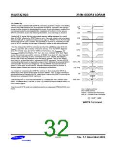
7.9.3 WRITEs
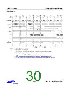
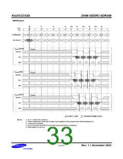
WRITE bursts are initiated with a WRITE command, as shown in Figure. The starting
column and bank addresses are provided with the WRITE command, and auto pre-
charge is either enabled or disabled for that access. If auto precharge is enabled, the
row being accessed is precharged at the completion of the burst. For the generic
WRITE commands used in the following illustrations, auto precharge is disabled.
/CK
CK
HIGH
CKE
During WRITE bursts, the first valid data-in element will be registered in a rising
edge of WDQS following the WRITE latency set in the mode register and subsequent
data elements will be registered on successive edges of WDQS. Prior to the first valid
WDQS edge a half cycle is needed and specified as the WRITE Preamble; the half
cycle in WDQS following the last data-in element is known as the write postamble.
/CS
/RAS
/CAS
/WE
The time between the WRITE command and the first valid falling edge of WDQS
(tDQSS) is specified with a relative to the write latency. All of the WRITE diagrams
show the nominal case, and where the two extreme cases (i.e., tDQSS(min) and
tDQSS(max)) might not be intuitive, they have also been included. Write Burst figure
shows the nominal case and the extremes of tDQSS for a burst of 4. Upon comple-
tion of a burst, assuming no other commands have been initiated, the DQs will
remain High-Z and any additional input data will be ignored. Data for any WRITE
burst may not be truncated with a subsequent WRITE command. The new WRITE
command can be issued on any positive edge of clock following the previous WRITE
command after the burst has completed. The new WRITE command should be
issued x cycles after the first WRITE command should be equals the number of
desired nibbles (nibbles are required by 4n-prefetch architecture).
A0-A7, A9
CA
A10, A11
A8
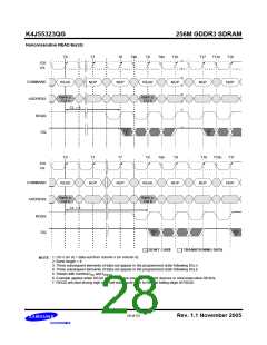
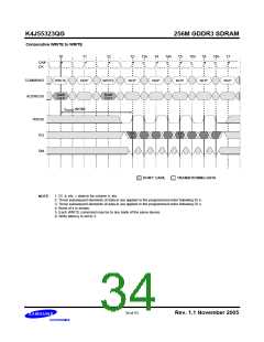
An example of nonconsecutive WRITEs is shown in Nonconsecutive WRITE to
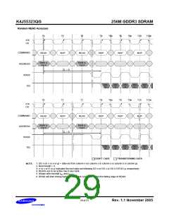
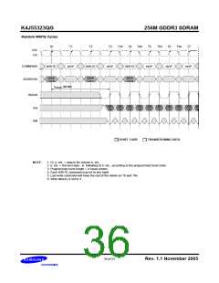
READ figure. Full-speed random write accesses within a page or pages can be per-
formed as shown in Random WRITE cycles figure. Data for any WRITE burst may be
followed by a subsequent READ command.
EN AP
DIS AP
BA
BA0, BA1
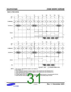
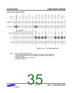
Data for any WRITE burst may be followed by a subsequent PRECHARGE com-
mand. To follow a WRITE the WRITE burst, tWR should be met as shown in WRITE to
PRECHARGE figure.
Data for any WRITE burst can not be truncated by a subsequent PRECHARGE com-
mand.
CA = Column Address
BA = Bank Address
EN AP = Enable Auto Precharge
DIS AP = Disable Auto Precharge
DON’T CARE
WRITE Command
32 of 53
Rev. 1.1 November 2005

 SAMSUNG [ SAMSUNG ]