256M GDDR3 SDRAM
K4J55323QG
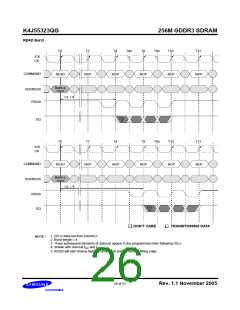
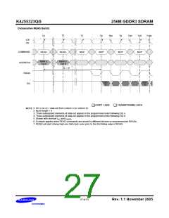
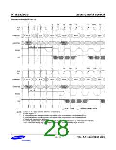
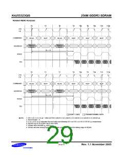
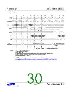
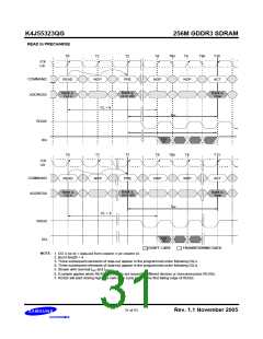
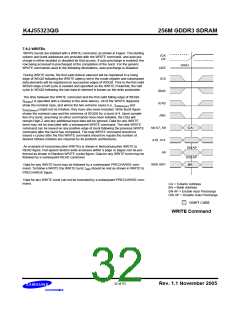
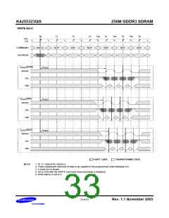
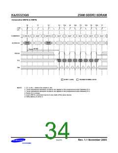
READ to WRITE
T0
T7
T8
T8n
T9
T9n
T10
T11
T12
T12n
/CK
CK
READ
NOP
WRITE
NOP
NOP
NOP
NOP
COMMAND
ADDRESS
RDQS
Bank
Col n
Bank a,
Col b
CL = 8
t
= 4
WL
WDQS
DQ
DI
b
DO
n
DM
DQ
DQ Termination Enbaled
1tCK <
DQ Termination Disabled
Termination
DON’T CARE
TRANSITIONING DATA
1. DO n = data-out from column n.
2. DI b = data-in from column b.
3. Burst length = 4
NOTE :
4. One subsequent element of data-out appears in the programmed order following DO n.
5. Data-in elements are applied following DI b in the programmed order.
6. Shown with nominal tAC and tDQSQ.
7. tDQSS in nominal case.
8. RDQS will start driving high one half-clock cycle prior to the first falling edge of RDQS.
9. The gap between data termination enable to the first data-in should be greater than 1tCK
30 of 53
Rev. 1.1 November 2005

 SAMSUNG [ SAMSUNG ]