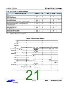
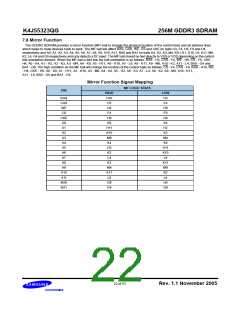
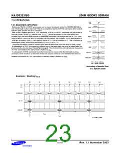
256M GDDR3 SDRAM
K4J55323QG
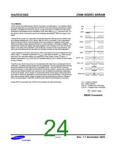
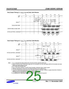
Data Output Timing (1) - t
, t and Data Valid Window
DQSQ QH
T0
T1
T2
T2n
T3
T3n
T4
CK#
CK
tCH
tDQSQ2 (MAX)
tDQSQ2 (MIN)
tCL
tDQSQ2 (MAX)
tDQSQ2 (MIN)
RDQS 1.6
4
4
tDQSH
tDQSL
DQ(Last data valid)
T2
T2n
T3
T3n
DQ(First data no longer valid)
All DQs and RDQS, collectively5
T2
T2
T2n
T3
T3n
T3
T3n
T2n
4
4
4
4
tDV
tDV
tDV
tDV
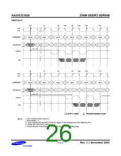
Data Output Timing (2) - t
, t and Data Valid Window
DQSQ QH
T0
T1
T2
T2n
T3
T3n
T4
CK#
CK
tCH
tCL
tAC(MAX)
RDQS 1.6
4
4
tDQSH
T2n
tDQSL
T3
All DQs and RDQS, collectively5
T2
T3n
tAC(MIN)
RDQS 1.6
4
4
tDQSH
T2n
tDQSL
T3
All DQs and RDQS, collectively5
T2
T3n
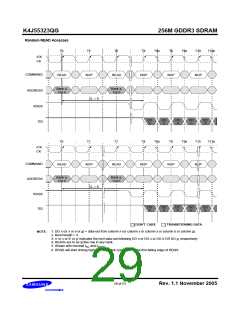
Note : 1. tDQSQ represents the skew between the 8 DQ lines and the respective RDQS pin.
2. tDQSQ is derived at each RDQS clock edge and is not cumulative over time and begins with first DQ transition and ends
with the last valid transition of DQs.
3. tAC is show in the nominal case
4. tDQHP is the lesser of tDQSL or tDQSH strobe transition collectively when a bank is active.
5. The data valid window is derived for each RDQS transitions and is defined by tDV
.
6. There are 4 RDQS pins for this device with RDQS0 in relation to DQ0-DQ7, RDQS1 in relation DQ8-DQ15, RDQS2 in
relation to DQ16-24 and RDQS3 in relation to DQ25-DQ31.
7. This diagram only represents one of the four byte lanes.
8. tAC represents the relationship between DQ, RDQS to the crossing of CK and /CK.
25 of 53
Rev. 1.1 November 2005

 SAMSUNG [ SAMSUNG ]