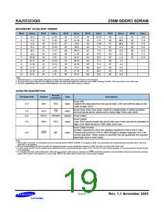
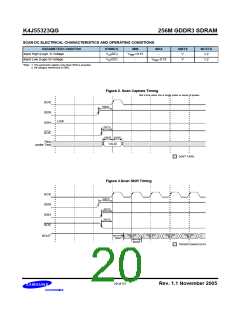
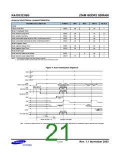
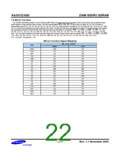
256M GDDR3 SDRAM
K4J55323QG
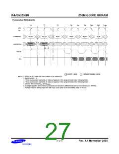
7.9 OPERATIONS
/CK
CK
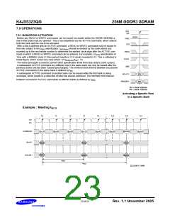
7.9.1 BANK/ROW ACTIVATION
HIGH
Before any READ or WRITE commands can be issued to a banks within the GDDR3 SDRAM, a
row in that bank must be “opened.” This is accomplished via the ACTIVE command, which selects
both the bank and the row to be activated.
CKE
/CS
After a row is opened with an ACTIVE command, a READ or WRITE command may be issued to
that row, subject to the tRCD specification. tRCD(min) should be divided by the clock period and
rounded up to the next whole number to determine the earliest clock edge after the ACTIVE com-
/RAS
/CAS
mand in which a READ or WRITE command can be entered. For example, a tRCD specification of
16ns with a 800MHz clock (1.25ns period) results in 12.8 clocks rounded to 13. This is reflected in
below figure, which covers any case where 12<tRCD(min)/tCK≤ 13.
The same procedure is used to convert other specification limits from time units to clock cycles).
A subsequent ACTIVE command to a different row in the same bank can only be issued after the
previous active row has been “closed”(precharged). The minimum time interval between successive
/WE
ACTIVE commands to the same bank is defined by tRC
.
A subsequent ACTIVE command to another bank can be issued while the first bank is being
A0-A11
BA0,BA1
RA
BA
accessed, which results in a reduction of total row access overhead. The minimum time interval
between successive ACTIVE commands to different banks is defined by tRRD
.
RA = Row Address
BA = Bank Address
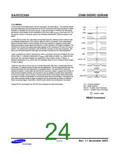
Activating a Specific Row
in a Specific Bank
Example : Meeting t
RCD
T0
T1
T2
T3
T4
T12
T13
T14
/CK
CK
COMMAND
ACT
RD/WR
Col
NOP
NOP
ACT
Row
NOP
NOP
NOP
A0-A11
Row
Bank x
BA0,BA1
Bank y
tRCD
Bank y
tRRD
DON’T CARE
23 of 53
Rev. 1.1 November 2005

 SAMSUNG [ SAMSUNG ]