256M GDDR3 SDRAM
K4J55323QG
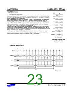
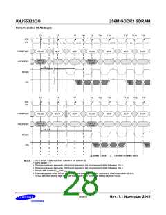
7.9.2 READs
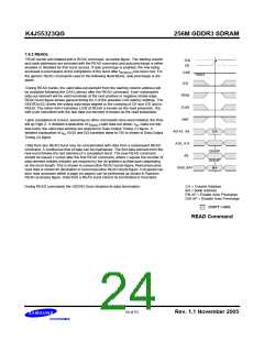
READ bursts are initiated with a READ command, as below figure. The starting column
and bank addresses are provided with the READ command and auto precharge is either
enabled or disabled for that burst access. If auto precharge is enabled, the row being
accessed is precharged at the completion of the burst after tRAS(min) has been met. For
the generic READ commands used in the following illustrations, auto precharge is dis-
abled.
/CK
CK
CKE
HIGH
/CS
/RAS
/CAS
/WE
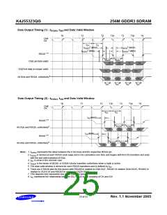
During READ bursts, the valid data-out element from the starting column address will
be available following the CAS Latency after the READ command. Each subsequent
data-out element will be valid nominally at the next positive or negative strobe edge.
READ burst figure shows general timing for 2 of the possible CAS latency settings. The
GDDR3(x32) drives the output data edge aligned to the crossing of CK and /CK and to
RDQS. The initial HIGH transition LOW of RDQS is known as the read preamble ; the
half cycle coincident with the last data-out element is known as the read postamble.
Upon completion of a burst, assuming no other commands have been initiated, the DQs
will go High-Z. A detailed explanation of tDQSQ (valid data-out skew), tDV (data-out win-
dow hold), the valid data window are depicted in Data Output Timing (1) figure. A
A0-A7, A9
A10, A11
A8
CA
detailed explanation of tAC (DQS and DQ transition skew to CK) is shown in Data Output
Timing (2) figure.
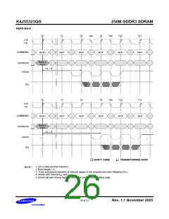
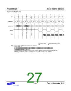
Data from any READ burst may be concatenated with data from a subsequent READ
command. A continuous flow of data can be maintained. The first data element from the
new burst follows the last element of a completed burst. The new READ command
should be issued x cycles after the first READ command, where x equals the number of
data element nibbles (nibbles are required by the 4n-prefetch architecture) depending
on the burst length. This is shown in consecutive READ bursts figure. Nonconsecutive
read data is shown for illustration in nonconsecutive READ bursts figure. Full-speed ran-
dom read accesses within a page (or pages) can be performed as shown in Random
READ accesses figure. Data from a READ burst cannot be terminated or truncated.
EN AP
DIS AP
BA
BA0, BA1
During READ commands the GDDR3 Dram disables its data terminators.
CA = Column Address
BA = Bank Address
EN AP = Enable Auto Precharge
DIS AP = Disable Auto Precharge
DON’T CARE
READ Command
24 of 53
Rev. 1.1 November 2005

 SAMSUNG [ SAMSUNG ]