256M GDDR3 SDRAM
K4J55323QG
SCAN AC ELECTRICAL CHARACTERISTICS
PARAMETER/CONDITON
Clock
SYMBOL
MIN
MAX
UNITS
NOTES
Clock cycle time
tSCK
40
-
ns
1
Scan Command Time
Scan enable setup time
Scan enable hold time
Scan command setup time for SSH, SOE# and SOUT
Scan command hold time for SSH, SOE# and SOUT
Scan Capture Time
tSES
tSEH
tSCS
tSCH
20
20
14
14
-
-
-
-
ns
ns
ns
ns
1,2
1
1
1
Scan capture setup Time
Scan capture hold Time
tSDS
tSCH
10
10
-
-
ns
ns
1
1
Scan Shift Time
Scan clock to valid scan output
Scan clock to scan output hold
tSAC
tSOH
-
6
-
ns
ns
1
1
1.5
*Note : 1. The parameter applies only when SEN is asserted.
2. Scan Enable should be issued earlier than other Scan Commands by 3ns.
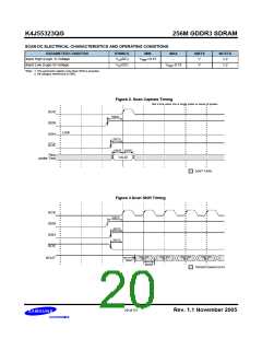
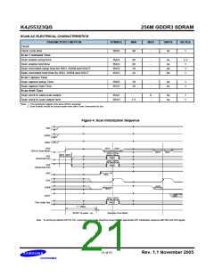
Figure 4. Scan Initialization Sequence
VDD
VDDQ
VREF
RES
tSCS
tSCH
(SSH in Scan Mode)
tSCS
tSCH
tSDS tSDH
tATS tATS
CKE
(Dual-load C/A)
VALID
tSDS tSDH
CKE
(Quad-load C/A)
VALID
SEN
SCK
tSES
tSCS
SOE#
tSCS
Scan Out
Bit0
SOUT
tSDS tSDH
VALID
Pins Under Test
T = 200us
RESET at power - up
Boundary Scan Mode
Note : To set the pre-defined ODT for C/A, a boundary scan mode should be issued after an appropriate ODT initialization sequence with RES and CKE signals
21 of 53
Rev. 1.1 November 2005

 SAMSUNG [ SAMSUNG ]