256M GDDR3 SDRAM
K4J55323QG
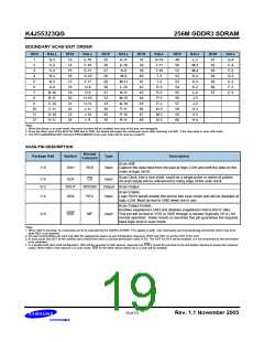
BOUNDARY SCAN EXIT ORDER
BIT#
1
2
3
4
5
6
7
8
BALL
D-3
C-2
C-3
B-2
BIT#
13
14
15
16
17
18
19
20
21
22
23
24
BALL
E-10
F-10
E-11
G-10
F-11
G-9
BIT#
25
26
27
28
29
30
31
32
33
34
35
36
BALL
K-11
K-10
K-9
BIT#
37
38
39
40
41
42
43
44
45
46
47
48
BALL
R-10
T-11
T-10
T-3
BIT#
49
50
51
52
53
54
55
56
57
58
59
60
BALL
L-3
BIT#
61
62
63
64
65
66
67
BALL
G-4
F-4
M-2
M-4
K-4
K-3
K-2
L-4
J-3
J-2
H-2
H-3
H-4
F-2
M-9
G-3
E-2
F-3
B-3
A-4
M-11
L-10
N-11
M-10
N-10
P-11
P-10
R-11
T-2
R-3
R-2
P-3
B-10
B-11
C-10
C-11
D-10
D-11
H-9
E-3
H-10
H-11
J-11
J-10
L-9
9
P-2
10
11
12
N-3
M-3
N-2
*Note :
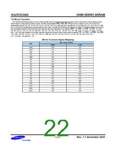
1. When the device is in scan mode, the mirror function will be disabled and none of the pins are remapped.
2. Since the other input of the MUX for DM0 tied to GND, the device will output the continuous zeros after scanning a bit #67, if the chip stays in scan shift mode.
3. Two RFU balls(#56and #57) and one RFM ball(#20) in the scan order will be read as a logic”0".
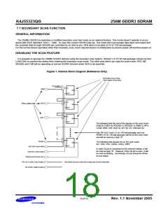
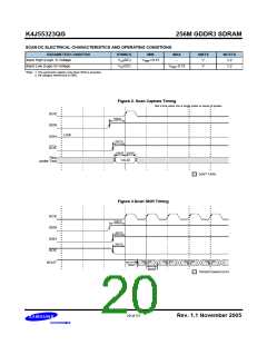
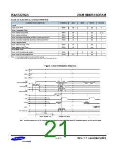
SCAN PIN DESCRIPTION
Normal
Package Ball
Symbol
Type
Input
Input
Description
Function
Scan shift.
V-9
SSH
RES
Capture the data input from the pad at logic LOW and shift the data on the
chain at logic HIGH.
Scan Clock. Not a true clock, could be a single pulse or series of pulses.
All scan inputs will be referenced to rising edge of the scan clock.
F-9
D-2
SCK
CS
SOUT
WDQS0
Output Scan Output.
Scan Enable.
Input
Input
V-4
SEN
SOE
RFU
MF
Logic HIGH would enable the device into scan mode and will be disabled at
logic LOW. Must be tied to GND when not in use.
Scan Output Enable.
Enables (registered LOW) and disables (registered HIGH) SOUT data.
This pin will be tied to VDD or GND through a resistor (typically 1K Ω ) for
normal operation. Tester needs to overdrive this pin guarantee the required
input logic level in scan mode.
A-9
*Note :
1. When SEN is asserted, no commands are to be executed by the GDDR3 SDRAM. This applies to both user commands and manufacturing commands which may exist
while RES is de-asserted.
2. All scan functionalities are valid only after the appropriate power-up and initialization sequence. (RES and CKE, to set the ODT of the C/A)
3. In scan mode, the ODT for the address and control lines set to a nominal termination value of ZQ. The ODT for DQ’s will be disabled. It is not necessary for the termination
to be calibrated.
4. In a double-load clam-shell configuration, SEN will be asserted to both devices. Separate two SOE’s should be provided to top and bottom devices to access the scanned
output. When either of the devices is in scan mode, SOE for the other device which not in a scan will be disabled.
19 of 53
Rev. 1.1 November 2005

 SAMSUNG [ SAMSUNG ]