256M GDDR3 SDRAM
K4J55323QG
7.7 BOUNDARY SCAN FUNCTION
GENERAL INFORMATION
The 256Mb GDDR3 incorporates a modified boundary scan test mode as an optional feature. This mode doesn’t operate in accor-
dance with IEEE Standard 1149.1 - 1990. To save the current GDDR3 ball-out, this mode will scan parallel data input and output and
the scanned data through WDQS0 pin controlled by an add-on pin, SEN which is located at V4 of 136 ball package.
For the normal device operation other than boundary scan, there required device re-initialization by device power-off and then power-on.
DISABLING THE SCAN FEATURE
It is possible to operate the 256Mb GDDR3 without using the boundary scan feature. SEN(at V-4 of 136 ball package) should be tied
LOW(VSS) to prevent the device from entering the boundary scan mode. The other pins which are used for scan mode, RES, MF,
WDQS0 and CS# will be operating at normal GDDR3 function when SEN is de-asserted.
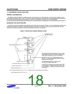
Figure 1. Internal Block Diagram (Reference Only)
Dedicated Scan Flops
(1per signal under test)
Tie to Iogic 0
D
DM0
DQ
CK
D
DQS
Pins under test
DQ
CK
D
DQ4
DQ
CK
The following lists the rest of the signals on the scan chain:
DQ[3:0], DQ[31:6], RDQS[3:1], WDQS[3:1], DM[3:1], RFU,
CAS#, WE#, CKE, BA[1:0], A[11:0], CK, CK# and ZQ
Two RFU’s(J-2 and J-3 on 136-ball package) and one
RFM(H-10 on 136-ball package) will be on the scan chain
and will be read as a logic "0"
D
RDQS0
The following lists signals not on the scan chain:
NC, VDD, VSS, VDDQ, VSSQ, VREF
DQ
CK
RES (SSH,Scan Shift)
In case ZQ pin is connected to the external resistor, it will
be read as logic "0". However, if the ZQ pin is open, it will
CS# (SCK, Scan Clock)
be read as floating. Accordingly, ZQ pin should be driven
by any signal.
WDQS0 (SOUT,Scan Out)
RFU at V-4 (SEN, Scan Enable)
MF (SOE#, Output Enable)
Puts device into scan mode and re-maps pins to scan functionality
18 of 53
Rev. 1.1 November 2005

 SAMSUNG [ SAMSUNG ]