64M DDR SDRAM
K4D623238B-GC
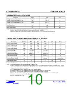
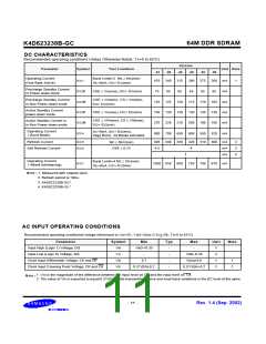
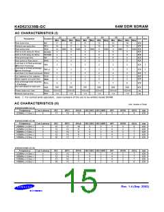
DC CHARACTERISTICS
Recommended operating conditions Unless Otherwise Noted, TA=0 to 65°C)
Version
Parameter
Symbol
Test Condition
Unit Note
-33
-40
-45
-50
-55
-60
Operating Current
(One Bank Active)
Burst Lenth=2 tRC ³ tRC(min)
IOL=0mA, tCC= tCC(min)
ICC1
470
340
315
290
275
260
mA
mA
mA
mA
mA
mA
1
Precharge Standby Current
in Power-down mode
ICC2P
ICC2N
ICC3P
ICC3N
ICC4
CKE £ VIL(max), tCC= tCC(min)
75
65
65
65
65
65
Precharge Standby Current
in Non Power-down mode
CKE ³ VIH(min), CS ³ VIH(min),
155
150
270
900
125
130
220
120
130
210
115
130
200
600
110
130
190
105
130
180
tCC= tCC(min)
Active Standby Current
power-down mode
CKE £ VIL(max), tCC= tCC(min)
CKE ³ VIH(min), CS ³ VIH(min),
Active Standby Current in
in Non Power-down mode
tCC= tCC(min)
Operating Current
( Burst Mode)
IOL=0mA ,tCC= tCC(min),
Page Burst, All Banks activated.
700
340
650
330
550
310
520
300
Refresh Current
ICC5
ICC6
405
4.5
320
4
mA
mA
mA
2
3
4
tRC ³ tRFC(min)
CKE £ 0.2V
Self Refresh Current
1
Operating Current
( 4Bank Interleaving)
Burst Lenth=4 tRC ³ tRC(min)
IOL=0mA, tCC= tCC(min)
ICC7
1050 850
800
750
700
670
mA
Note : 1. Measured with outputs open.
2. Refresh period is 16ms.
3. K4D623238B-GC*
4. K4D623238B-GL*
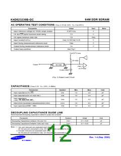
AC INPUT OPERATING CONDITIONS
Recommended operating conditions(Voltage referenced to VSS=0V, VDD/ VDDQ=2.5V+ 5%, TA=0 to 65°C)
Parameter
Symbol
VIH
Min
VREF+0.35
-
Typ
Max
Unit
Note
Input High (Logic 1) Voltage; DQ
-
-
-
-
-
V
V
V
V
Input Low (Logic 0) Voltage; DQ
VIL
VREF-0.35
VDDQ+0.6
Clock Input Differential Voltage; CK and CK
Clock Input Crossing Point Voltage; CK and CK
VID
0.7
1
2
VIX
0.5*VDDQ-0.2
0.5*VDDQ+0.2
1. VID is the magnitude of the difference between the input level on CK and the input level on CK
Note :
2. The value of VIX is expected to equal 0.5*VDDQ of the transmitting device and must track variations in the DC level of the same
- 11 -
Rev. 1.4 (Sep. 2002)

 SAMSUNG [ SAMSUNG ]