64M DDR SDRAM
K4D623238B-GC
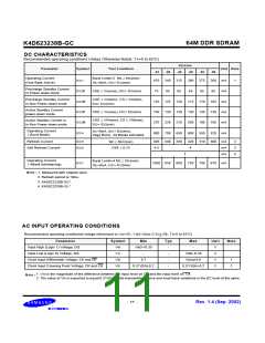
AC OPERATING TEST CONDITIONS (VDD=2.5V±0.125V, TA= 0 to 65°C)
Parameter
Value
0.50*VDDQ
1.5
Unit
V
Note
Input reference voltage for CK(for single ended)
CK and CK signal maximum peak swing
V
CK signal minimum slew rate
Input Levels(VIH/VIL)
1.0
V/ns
V
VREF+0.35/VREF-0.35
Input timing measurement reference level
Output timing measurement reference level
Output load condition
VREF
Vtt
V
V
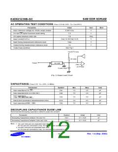
See Fig.1
Vtt=0.5*V DDQ
RT=50W
Output
Z0=50W
VREF
=0.5*VDDQ
CLOAD=30pF
(Fig. 1) Output Load Circuit
CAPACITANCE (VDD=3.3V, TA= 25°C, f=1MHz)
Parameter
Symbol
Min
Max
Unit
Input capacitance( CK, CK )
CIN1
1.0
5.0
pF
pF
Input capacitance(A0~A10, BA0~BA1)
CIN2
CIN3
1.0
1.0
4.0
4.0
Input capacitance
( CKE, CS, RAS,CAS, WE )
pF
Data & DQS input/output capacitance(DQ0~DQ31)
Input capacitance(DM0 ~ DM3)
COUT
CIN4
1.0
1.0
6.5
6.5
pF
pF
DECOUPLING CAPACITANCE GUIDE LINE
Recommended decoupling capacitance added to power line at board.
Parameter
Symbol
CDC1
Value
Unit
Decoupling Capacitance between VDD and VSS
Decoupling Capacitance between VDDQ and VSSQ
0.1 + 0.01
0.1 + 0.01
uF
uF
CDC2
Note :
1. VDD and VDDQ pins are separated each other.
All VDD pins are connected in chip. All VDDQ pins are connected in chip.
2. VSS and VSSQ pins are separated each other
All VSS pins are connected in chip. All VSSQ pins are connected in chip.
- 12 -
Rev. 1.4 (Sep. 2002)

 SAMSUNG [ SAMSUNG ]