64M DDR SDRAM
K4D623238B-GC
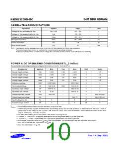
ABSOLUTE MAXIMUM RATINGS
Parameter
Voltage on any pin relative to Vss
Voltage on VDD supply relative to Vss
Voltage on VDD supply relative to Vss
Storage temperature
Symbol
VIN, VOUT
VDD
Value
-0.5 ~ 3.6
-1.0 ~ 3.6
-0.5 ~ 3.6
-55 ~ +150
2.0
Unit
V
V
VDDQ
TSTG
V
°C
W
Power dissipation
PD
Short circuit current
IOS
50
mA
Note :
Permanent device damage may occur if ABSOLUTE MAXIMUM RATINGS are exceeded.
Functional operation should be restricted to recommended operating condition.
Exposure to higher than recommended voltage for extended periods of time could affect device reliability.
POWER & DC OPERATING CONDITIONS(SSTL_2 In/Out)
Recommended operating conditions(Voltage referenced to VSS=0V, TA=0 to 65°C)
Parameter
Device Supply voltage
Output Supply voltage
Device Supply voltage
Output Supply voltage
Reference voltage
Symbol
VDD
VDDQ
VDD
VDDQ
VREF
Vtt
Min
2.375
2.375
2.66
Typ
Max
2.625
Unit
V
Note
2.50
1,7
2.50
2.625
V
1,7
2.8
2.94
V
1,8
2.66
2.8
2.94
V
1,8
0.49*VDDQ
VREF-0.04
VREF+0.15
-0.30
-
0.51*VDDQ
VREF+0.04
VDDQ+0.30
VREF-0.15
-
V
2
Termination voltage
VREF
V
3
Input logic high voltage
Input logic low voltage
Output logic high voltage
Output logic low voltage
Input leakage current
Output leakage current
VIH
-
-
-
-
-
-
V
4
VIL
V
5
VOH
VOL
Vtt+0.76
-
V
IOH=-15.2mA
Vtt-0.76
5
V
IOL=+15.2mA
IIL
-5
uA
uA
6
6
IOL
-5
5
1. Under all conditions VDDQ must be less than or equal to VDD.
Note :
2. VREF is expected to equal 0.50*VDDQ of the transmitting device and to track variations in the DC level of the same. Peak to
peak noise on the VREF may not exceed + 2% of the DC value. Thus, from 0.50*VDDQ, VREF is allowed + 25mV for DC error
and an additional + 25mV for AC noise.
3. Vtt of the transmitting device must track VREF of the receiving device.
4. VIH(max.)= VDDQ +1.5V for a pulse width and it can not be greater than 1/3 of the cycle rate.
5. VIL(mim.)= -1.5V for a pulse width and it can not be greater than 1/3 of the cycle rate.
6. For any pin under test input of 0V < VIN < VDD is acceptable. For all other pins that are not under test VIN=0V.
7. For -40/-45/-50/-55/-60, VDD/VDDQ=2.5V + 5%
8. For -33, VDD/VDDQ=2.8V + 5%
- 10 -
Rev. 1.4 (Sep. 2002)

 SAMSUNG [ SAMSUNG ]