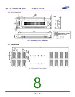
2X20 LCD Compatible VFD Module
20T202DA1E (Rev. 3.0)
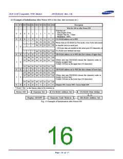
6. INSTRUCTIONS
6.1 Outline
Only the instruction register (IR) and the data register (DR) of the VFD controller can be controlled by the user's MPU.
Before starting the internal operation of the controller, control information is temporarily stored into these registers to
allow different data transfer mode, display line setting and dimming control etc. The internal operation of the controller
is determined by signals sent from the MPU. These signals, which include register selection signal (RS), write enable
signal (E), and the data bus (DB4 to DB7), make up the controller instructions.
There are four categories of instructions which are:
* Designate controller functions, such as display format, data length, etc.
* Set internal RAM addresses.
* Perform data transfer with internal RAM.
* Perform miscellaneous functions.
Normally, instructions that perform data transfer with internal RAM are used the most.
However, auto-incrementation by 1 (or auto-decrementation by 1) of internal RAM addresses after each data write can
lighten the program load of the MPU. Since the display shift instruction can perform concurrently with display data
write, the user can minimize system development time with maximum programming efficiency.
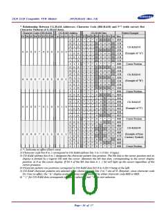
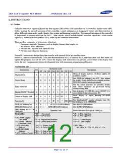
*Instruction List
Instruction Code
Instructions
RS
0
Descriptions
D7 D6 D5 D4 D3 D2 D1 D0
Clears all display and sets DD-RAM address 00
in address counter.
Display Clear
0
0
0
0
0
0
0
1
Sets DD-RAM address 0 in ACC. Also returns
the display being shifted to the original position.
DD-RAM contents remain unchanged.
Cursor Home
0
0
0
0
0
0
0
0
1
*
Sets the cursor direction and specifies display
shift. These operations are performed during
writing/reading data.
Entry Mode Set
0
0
0
0
0
1
1
I/D
S
Sets all display ON/OFF (D), cursor ON/OFF (C),
cursor blink of character position (B).
Display ON/OFF Control
Cursor or Display Shift
Function Set
0
0
0
0
0
0
0
0
0
0
1
0
1
D
C
*
B
*
Shifts display or cursor, keeping DD-RAM
contents.
S/C R/L
Sets data length (IF), number of display lines (N),
Set brightness level (BR1,BR0)
0
1
IF
N
*
BR1 BR0
CG-RAM Address Set
DD-RAM Address Set
0
1
0
1
ACG (CG-RAM Address)
Sets the CG-RAM address.
Sets the DD-RAM address.
ADD (DD-RAM Address)
Data Writing to CG- or
DD-RAM
1
Character Code
Writes data into CG-RAM or DD-RAM.
* I/D = 1: Increment
* I/D = 0: Decrement
* IF = 1: 8-bit Operation
* IF = 0: 4-bit Operation
REMARKS:
* DD-RAM: Display
Data RAM
* CG-RAM: Character
Generator RAM
* ACG: CG-RAM
Address
* S = 1: Display Shift Enabled
* S = 0: Cursor Shift Enabled
* N = 1: 2 Lines Display
* N = 0: 1 Line Display
* S/C = 1: Display Shift
* S/C = 0: Cursor Move
* BR1, BR0 =
00: 100%, 01: 75%, 10: 50%, 11: 25%
* ADD: DD-RAM
Address
* R/L = 1: Shift to the Right
* ACC: Address Counter * R/L = 0: Shift to the Left
Page - 12 of 17

 SAMSUNG [ SAMSUNG ]