2X20 LCD Compatible VFD Module
20T202DA1E (Rev. 3.0)
5. FUNCTION DESCRIPTIONS
5.1 Registers in VFD Controller
The VFD controller has two 8-bit registers, an instruction register (IR) and a data register (DR). IR stores instruction
codes, such as display clear and cursor shift, and address information for DD-RAM and CG-RAM. The IR can only be
written from the host MPU. DR temporarily stores data to be written into DD-RAM or CG-RAM and temporarily
stores data to be read from DD-RAM or CG-RAM. Data written into the DR from the MPU is automatically written
into DD-RAM or CG-RAM by an internal operation. The DR is also used for data storage when reading data from
DD-RAM or CG-RAM. When address information is written into the IR, data is read and then stored into the DR from
DD-RAM or CG-RAM by internal operation. Data transfer between MPU is then completed when the MPU reads the
DR. After the read, data in DD-RAM or CG-RAM at the next address is sent to the DR for the next read from the MPU.
By the register selector (RS) signal, these two registers can be selected.
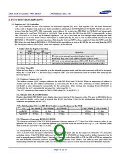
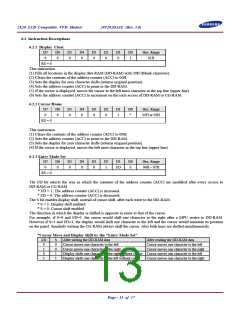
* Truth Table for Register Selection
M68
R/W
0
1
0
1
i80
RS
Operation
/RD
1
0
1
0
/WR
0
0
1
1
0
1
0
1
IR write as an internal operation (display clear, etc.)
Read busy flag (DB7) and address counter (DB0 to DB6)
DR write as an internal operation (DR to DD-RAM or CG-RAM)
DR read as an internal operation (DD-RAM or CG-RAM to DR)
5.1.1 Busy Flag (BF)
When the busy flag is 1, the controller is in the internal operation mode, and the next instruction will not be accepted.
When RS = 0 and R/W = 1, the busy flag is output to DB7. The next instruction must be written after ensuring that
the busy flag is 0.
5.1.2 Address Counter (ACC)
The address counter (ACC) assigns addresses for both DD-RAM and CG-RAM. When an instruction of address is
written into the IR, the address information is sent from the IR to the ACC. Selection of either DD-RAM or
CG-RAM is also determined concurrently by the instruction. After writing into (reading from) DD-RAM or
CG-RAM, the ACC automatically increased by 1 (decreased by 1).
The ACC contents are then output to DB0 to DB6 when RS = 0 and R/W = 1.
5.1.3 Display Data RAM (DD-RAM)
Display data RAM (DD-RAM) stores display data represented in 8-bit character codes. The area in DD-RAM that is
not used for display can be used as general data RAM. See below Table for the relationships between DD-RAM
addresses and positions on the VFD.
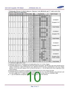
* The Relationships Between DD-RAM Addresses and Positions on the VFD
1st Column
00 Hex
2nd Column
01 Hex
3rd Column
02 Hex
………
………
………
19th Column 20th Column
1st ROW
2nd ROW
12 Hex
52 Hex
13 Hex
53 Hex
40 Hex
41Hex
42 Hex
5.1.3 Character Generator ROM (CG-ROM)
The character generator ROM (CG-ROM) generates character patterns of 5*7 dots from 8-bit character codes. It can
generate 240 kinds of 5*7 dot character patterns. The character fonts are shown on the Fig.-10. The character codes
00H to 0FH are allocated to the CG-RAM.
5.1.4 Character Generator RAM (CG-RAM)
The CG-RAM stores the pixel information (1=pixel on, 0=pixel off) for the eight user-definable 5*7 characters
including cursor. Valid CG-RAM addresses are 00H to 3FH. CG-RAM not being used to define characters can be
used as general purpose RAM (lower 5 bits only). Character codes from 00H to 07H (or 08H to 0FH) are assigned to
the user-definable characters (refer to Appendix-1 for Character Font Tables). The table on next page shows the
relationship between the character codes, CG-RAM addresses, and CG-RAM data for each user-definable character.
Page - 9 of 17

 SAMSUNG [ SAMSUNG ]