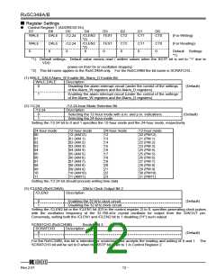
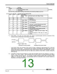
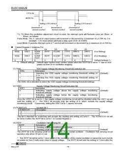
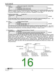
Rx5C348A/B
(5) /CLEN1
32kHz Clock Output Bit 1 (Rx5C348A)
Description
/CLEN1
0
1
Enabling the 32-kHz clock circuit
Disabling the 32-kHz clock circuit
(Default)
Setting the /CLEN1 bit or the /CLEN2 bit (D4 in the control register 1) to 0, specifies generating clock pulses
with the oscillation frequency of the 32.768-kHz crystal oscillator for output from the 32KOUT pin.
Conversely, setting both the /CLEN1 and /CLEN2 bit to 1 disabling (”H”) such output.
SCRATCH2 (Rx5C348B)
Scratch Bit 2
SCRATCH2
Description
0
1
(Default)
For the Rx5C348B, this bit is intended for scratching and accepts the reading and writing of 0 and 1. The
SCRATCH3 bit will be set to 0 when the XSTP bit is set to 1 in Control Register 2.
(6) CTFG
Periodic Interrupt Flag Bit
Description
CTFG
0
1
Periodic interrupt output = “H”
Periodic interrupt output = “L”
(Default)
The CTFG bit is set to 1 when the periodic interrupt signals are output from the /INTR pin (“L”). The CTFG
bit accepts only the writing of 0 in the level mode, which disables (“H”) the /INTR pin until it is enabled (“L”)
again in the next interrupt cycle. Conversely, setting the CTFG bit to 1 causes no event.
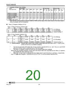
(7) WAFG,DAFG
Alarm_W Flag Bit and Alarm_D Flag Bit
WAFG,DAFG
Description
0
1
Indicating a mismatch between current time and preset alarm time
Indicating a match between current time and preset alarm time
(Default)
The WAFG and DAFG bits are valid only when the WALE and DALE have the setting of 1, which is caused
approximately 61µs after any match between current time and preset alarm time specified by the Alarm_W
registers and the Alarm_D registers. The WAFG (DAFG) bit accepts only the writing of 0. /INTR pin
outputs off (“H”) when this bit is set to 0. And /INTR pin outputs “L” again at the next preset alarm time.
Conversely, setting the WAFG and DAFG bits to 1 causes no event. The WAFG and DAFG bits will have
the reading of 0 when the alarm interrupt circuit is disabled with the WALE and DALE bits set to 0. The
settings of the WAFG and DAFG bits are synchronized with the output of the /INTR pin as shown in the
timing chart below.
Approx. 61µs
Approx. 61µs
WAFG(DAFG) Bit
/INTR Pin
Writing of 0 to
Writing of 0 to
WAFG(DAFG) bit
WAFG(DAFG) bit
(Match between
(Match between
(Match between
current time and
current time and
current time and
preset alarm time)
preset alarm time)
preset alarm time)
12345
Rev.2.01
- 16 -

 RICOH [ RICOH ELECTRONICS DEVICES DIVISION ]