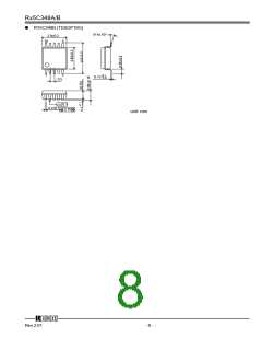
Rx5C348A/B
ꢀ Register Settings
ꢁ
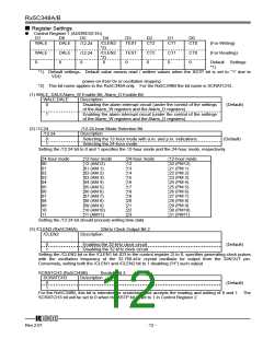
Control Register 1 (ADDRESS Eh)
D7
WALE
D6
DALE
D5
/12⋅24
D4
/CLEN2
*2)
D3
TEST
D2
CT2
D1
CT1
D0
CT0
(For Writing)
WALE
0
DALE
0
/CLEN2
*2)
0
TEST
0
CT2
0
CT1
0
CT0
0
(For Reading)
/12⋅24
0
Default Settings
*1)
*1) Default settings: Default value means read / written values when the XSTP bit is set to “1” due to
VDD
power-on from 0v or oscillation stopping
*2) This bit name applies to the Rx5C348A only. For the Rx5C348B the bit name is SCRATCH3..
(1) WALE, DALEAlarm_W Enable Bit, Alarm_D Enable Bit
WALE,DALE
0
Description
Disabling the alarm interrupt circuit (under the control of the settings
of the Alarm_W registers and the Alarm_D registers).
Enabling the alarm interrupt circuit (under the control of the settings
of the Alarm_W registers and the Alarm_D registers)
(Default)
1
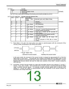
(2) /12⋅24
/12-24-hour Mode Selection Bit
Description
/12⋅24
0
1
Selecting the 12-hour mode with a.m. and p.m. indications.
Selecting the 24-hour mode
(Default)
Setting the /12⋅24 bit to 0 and 1 specifies the 12-hour mode and the 24-hour mode, respectively.
24-hour mode
12-hour mode
12 (AM12)
01 (AM 1)
02 (AM 2)
03 (AM 3)
04 (AM 4)
05 (AM 5)
06 (AM 6)
07 (AM 7)
08 (AM 8)
09 (AM 9)
10 (AM10)
11 (AM11)
24-hour mode
12-hour mode
32 (PM12)
21 (PM 1)
22 (PM 2)
23 (PM 3)
24 (PM 4)
25 (PM 5)
26 (PM 6)
27 (PM 7)
28 (PM 8)
29 (PM 9)
30 (PM10)
31 (PM11)
00
01
02
03
04
05
06
07
08
09
10
11
12
13
14
15
16
17
18
19
20
21
22
23
Setting the /12⋅24 bit should precede writing time data
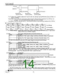
(3) /CLEN2 (Rx5C348A)
/CLEN2
32kHz Clock Output Bit 2
Description
0
1
Enabling the 32-kHz clock circuit
Disabling the 32-kHz clock circuit
(Default)
Setting the /CLEN2 bit or the /CLEN1 bit (D3 in the control register 2) to 0, specifies generating clock pulses
with the oscillation frequency of the 32.768-kHz crystal oscillator for output from the 32KOUT pin.
Conversely, setting both the /CLEN1 and /CLEN2 bit to 1 disabling (”H”) such output.
SCRATCH3 (Rx5C348B)
Scratch Bit 3
SCRATCH3
Description
0
1
(Default)
For the Rx5C348B, this bit is intended for scratching and accepts the reading and writing of 0 and 1. The
SCRATCH3 bit will be set to 0 when the XSTP bit is set to 1 in Control Register 2.
12345
Rev.2.01
- 12 -

 RICOH [ RICOH ELECTRONICS DEVICES DIVISION ]