Rx5C348A/B
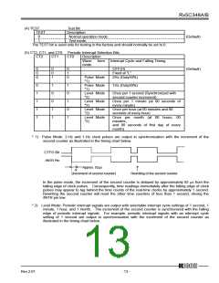
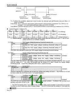
CTFG Bit
/INTR Pin
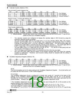
Setting CTFG bit to 0
Setting CTFG bit to 0
(Increment of
second counter)
(Increment of
second counter)
(Increment of
second counter)
*1), *2) When the oscillation adjustment circuit is used, the interrupt cycle will fluctuate once per 20sec. or
60sec. as follows:
Pulse Mode: The “L” period of output pulses will increment or decrement by a maximum of ±3.784 ms. For
example, 1-Hz clock pulses will have a duty cycle of 50 ±0.3784%.
Level Mode: A periodic interrupt cycle of 1 second will increment or decrement by a maximum of ±3.784 ms.
ꢁ
Control Register 2 (Address Fh)
D7
D6
D5
D4
D3
D2
D1
D0
VDSL
VDET
SCRA
TCH1
SCRA
TCH1
0
XSTP
/CLEN1
CTFG
WAFG
DAFG
(For Writing)
VDSL
VDET
XSTP
/CLEN1
CTFG
WAFG
DAFG
(For Reading)
0
0
1
0
0
0
0
Default Settings *)
*) Default settings: Default value means read / written values when the XSTP bit is set to “1” due to VDD
power-on from 0v or oscillation stopping
(1) VDSL
VDD Supply Voltage Monitoring Threshold Selection Bit
VDSL
0
Description
Selecting the VDD supply voltage monitoring threshold setting of
(Default)
2.1v.
1
Selecting the VDD supply voltage monitoring threshold setting of
1.6v.
The VDSL bit is intended to select the VDD supply voltage monitoring threshold settings.
(2) VDET
Supply Voltage Monitoring Result Indication Bit
Description
Indicating supply voltage above the supply voltage monitoring
threshold settings.
VDET
0
(Default)
1
Indicating supply voltage below the supply voltage monitoring
threshold settings.
Once the VDET bit is set to 1, the supply voltage monitoring circuit will be disabled while the VDET bit will
hold the setting of 1. The VDET bit accepts only the writing of 0, which restarts the supply voltage
monitoring circuit. Conversely, setting the VDET bit to 1 causes no event.
(3) SCRATCH1
Scratch Bit 1
Description
SCRATCH1
0
1
(Default)
This bit is intended for scratching and accepts the reading and writing of 0 and 1. The SCRATCH1 bit will
be set to 0 when the XSTP bit is set to 1 in Control Register 2.
(4) XSTP
Oscillation Halt Sensing Bit
Description
XSTP
0
1
Sensing a normal condition of oscillation
Sensing a halt of oscillation
(Default)
The XSTP bit is for sensing a halt in the oscillation of the crystal oscillator. Oscillation Halt sensing circuit
operates only when CE pin is Low.
* The XSTP bit will be set to 1 once a halt in the oscillation of the crystal oscillator is caused by such events
as power-on from 0 volts and a drop in supply voltage. The XSTP bit will hold the setting of 1 even after the
12345
Rev.2.01
- 14 -

 RICOH [ RICOH ELECTRONICS DEVICES DIVISION ]