Rx5C348A/B
cause neither an increment nor decrement of time counts.
Example:
When the second digits read 00, 20, or 40, the settings of "0, 0, 0, 0, 1, 1, 1" in the F6, F5, F4, F3, F2, F1,
and F0 bits cause an increment of the current time counts of 32768 by (7 - 1) x 2 to 32780 (a current time
count loss). When the second digits read 00, 20, or 40, the settings of "0, 0, 0, 0, 0, 0, 1" in the F6, F5, F4,
F3, F2, F1, and F0 bits cause neither an increment nor a decrement of the current time counts of 32768.
When the second digits read 00, 20, or 40, the settings of "1, 1, 1, 1, 1, 1, 0" in the F6, F5, F4, F3, F2, F1,
and F0 bits cause a decrement of the current time counts of 32768 by (- 2) x 2 to 32764 (a current time
count gain).
An increase of two clock pulses once per 20 seconds causes a time count loss of approximately 3 ppm (2 /
(32768 x 20 = 3.051 ppm). Conversely, a decrease of two clock pulses once per 20 seconds causes a time
count gain of 3 ppm. Consequently, deviations in time counts can be corrected with a precision of ±1.5
ppm. Note that the oscillation adjustment circuit is configured to correct deviations in time counts and not
the oscillation frequency of the 32.768-kHz clock pulses. For further details, see "P.30 ꢁOscillation
Adjustment Circuit".
ꢁ
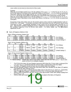
Alarm_W Registers (Address 8-Ah)
Alarm_W Minute Register (Address 8h)
D7
D6
D5
D4
D3
D2
D1
D0
-
WM40
WM20
WM10
WM8
WM4
WM2
WM1
(For Writing)
0
0
WM40
Indefinite
WM20
Indefinite
WM10
Indefinite
WM8
Indefinite
WM4
Indefinite
WM2
Indefinite
WM1
Indefinite
(For Reading)
Default Settings *)
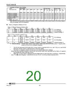
Alarm_W Hour Register (Address 9h)
D7
D6
D5
D4
D3
D2
D1
D0
-
-
WH20
WP⋅/A
WH20
WP⋅/A
Indefinite
WH10
WH8
WH4
WH2
WH1
(For Writing)
0
0
0
0
WH10
WH8
WH4
WH2
WH1
(For Reading)
Default Settings *)
Indefinite
Indefinite
Indefinite
Indefinite
Indefinite
Alarm_W Day-of-week Register (Address Ah)
D7
D6
D5
D4
D3
D2
D1
D0
-
WW6
WW5
WW4
WW3
WW2
WW1
WW0
(For Writing)
0
0
WW6
Indefinite
WW5
Indefinite
WW4
Indefinite
WW3
Indefinite
WW2
Indefinite
WW1
Indefinite
WW0
Indefinite
(For Reading)
Default Settings *)
*) Default settings: Default value means read / written values when the XSTP bit is set to “1” due to VDD
power-on from 0v or oscillation stopping
*
*
The D5 bit of the Alarm_W Hour Register represents WP/A when the 12-hour mode is selected (0 for
a.m. and 1 for p.m.) and WH20 when the 24-hour mode is selected (tens in the hour digits).
The Alarm_W Registers should not have any non-existent alarm time settings.
(Note that any mismatch between current time and preset alarm time specified by the Alarm_W registers
may disable the alarm interrupt circuit.)
*
*
*
When the 12-hour mode is selected, the hour digits read 12 and 32 for 0 a.m. and 0 p.m., respectively.
(See "P12 ꢁControl Register 1 (ADDRESS Eh) (2) /12⋅24: 12-/24-hour Mode Selection Bit")
WW0 to WW6 correspond to W4, W2, and W1 of the day-of-week counter with settings ranging from
(0, 0, 0) to (1, 1, 0).
WW0 to WW6 with respective settings of 0 disable the outputs of the Alarm_W Registers.
12345
Rev.2.01
- 19 -

 RICOH [ RICOH ELECTRONICS DEVICES DIVISION ]