RT8876A
Thermal Monitoring and Temperature Reporting
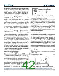
The VRHOT pin is an open-drain structure that sends out
active-low VRHOT signal. When b6 of Temperature_Zone
register asserts to 1 (when TSENA voltage rises above
1.79V), theALERT signal will be asserted to low, which is
so-called SVID thermal alert. In the mean time, the AXG
VR will assert the bit 1 data to 1 in Status_1 register. The
ALERT assertion will be de-asserted when b5 of
Temperature_Zone register is de-asserted from 1 to 0
(which means TSENA voltage falls under 1.735V), and
the bit 1 of Status_1 register will also be cleared to 0. The
bit 1 assertion of Status_1 is not latched and cannot be
cleared byGetReg command.
The AXG VR provides thermal monitoring function via
sensing TSENA pin voltage. Through the voltage divider
resistors, R1 and RNTC, the voltage of TSENA will be
proportional to VR temperature. When VR temperature
rises, the TSENA voltage also rises. The ADC circuit of
theAXGVR monitors the voltage variation at the TSENA
pin from 1.46V to 1.845V with 55mV resolution. This
voltage is then decoded into digital format and stored into
Temperature_Zone register. To meet Intel's VR12/IMVP7
specification, platform users have to set the TSENA voltage
to meet the temperature variation of VR from 75% to 100%
VR max temperature.
When b7 of Temperature_Zone register asserts to 1 (when
TSENA voltage rises above 1.845V), the VRHOT signal
will be asserted to low. The VRHOT assertion will be de-
asserted when b6 of Temperature_Zone register is de-
asserted from 1 to 0 (which means TSENA voltage falls
under 1.79V). The thermal monitoring function of theAXG
VR can be disabled by connecting TSENA to VCC5. If
TSENA is disabled, all the SVID commands related to
Tmperature_Zone register of theAXGVR will be rejected.
For example, if the VR max temperature is 100°C, platform
users have to set the TSENA voltage to be 1.46V when
VR temperature reaches 75°C and 1.845V when VR
temperature reaches 100°C.Detailed voltage setting versus
temperature variation is shown in Table 5. The thermometer
code is implemented in Temperature_Zone register.
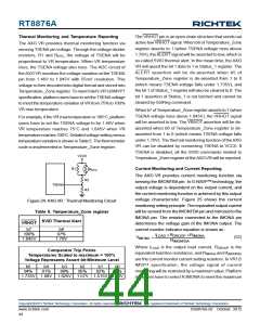
VCC5
R1
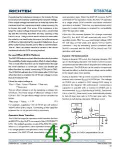
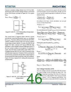
Current Monitoring and Current Reporting
R
NTC
The AXG VR provides current monitoring function via
sensing the IMONFBA pin. In G-NAVPTM technology, the
output voltage is dependent on the output current, and
the current monitoring function is achieved by this output
voltage characteristic. Figure 25 shows the current
monitoring setting principle. The equivalent output current
will be sensed from the IMONFBApin and mirrored to the
IMONA pin. The resistor connected to the IMONA pin
determines the voltage gain of the IMONA output. The
current monitor indicator equation is shown as :
R2
R3
TSENA
Figure 24. AXGVR : Thermal Monitoring Circuit
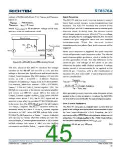
Table 5. Temperature_Zone register
SVID Thermal Alert
VRHOT
b7
b6
100%
1.845V
97%
1.79V
I
×R
R
×R
LOAD
DROOP IMONA
(52)
V
IMONA
=
IMONFBA
Where ILOAD is the output load current, RDROOP is the
equivalent load line resistance, and RIMONA and RIMONFBA
are the current monitor current setting resistors. In VR12/
IMVP7 specification, the voltage signal of current
monitoring will be restricted by a maximum value. Platform
designers have to select R IMONA to meet the maximum
Comparator Trip Points
Temperatures Scaled to maximum = 100%
Voltage Represents Assert bit Minimum Level
b5
94%
b4
b3
b2
b1
82%
b0
75%
91%
88%
85%
1.735V 1.68V 1.625V 1.57V 1.515V 1.46V
Copyright 2012 Richtek Technology Corporation. All rights reserved.
©
is a registered trademark of Richtek Technology Corporation.
www.richtek.com
44
DS8876A-02 October 2012

 RICHTEK [ RICHTEK TECHNOLOGY CORPORATION ]