RT8876A
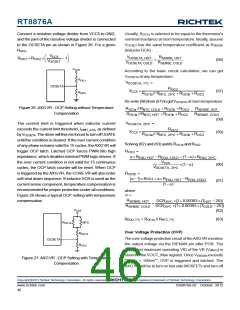
high side MOSFETs of the AXG VR to protect the CPU.
When OVP is triggered by the AXG VR, the CORE VR
will also enter shut down sequence. A 1μs delay is used
in OVP detection circuit to prevent false trigger. Note that
if OFSA pin is higher than 0.9V before power up, OVP
would trigger when “V(MAX) + 850mV”.
Output LC Filter
Inductor Selection
The switching frequency and ripple current determine the
inductor value as follows :
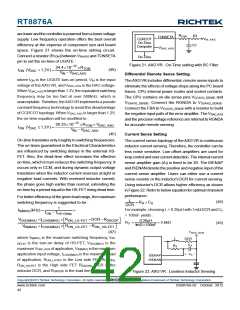
V
IN − VOUT
LMIN
=
× TON
(64)
IRipple(MAX)
Negative Voltage Protection (NVP)
where TON is the UGATE turn-on period. Higher inductance
yields in less ripple current and hence higher efficiency.
The downside is a slower transient response of the power
stage to load transients. This might increase the need for
more output capacitors, thus driving up the cost. Select a
low loss inductor having the lowest possibleDC resistance
that fits in the allotted dimensions. The core must be large
enough not to be saturated at the peak inductor current.
During OVP latch state, the AXG VR also monitors the
ISENAN pin for negative voltage protection. Since the OVP
latch continuously turns on all low side MOSFETs of the
AXGVR, theAXGVR may suffer negative output voltage.
As a consequence, when the ISENAN voltage drops below
−0.05V after triggering OVP, theAXGVR will triggerNVP
to turn off all low side MOSFETs of theAXGVR while the
high side MOSFETs remains off. After triggering NVP, if
the output voltage rises above 0V, the OVP latch will restart
to turn on all low side MOSFETs.
Output Capacitor Selection
Output capacitors are used to obtain high bandwidth for
the output voltage beyond the bandwidth of the converter
itself. Usually, the CPU manufacturer recommends a
capacitor configuration. Two different kinds of output
capacitors are typically used : bulk capacitors closely
located next to the inductors, and ceramic output
capacitors in close proximity to the load. Latter ones are
for mid-frequency decoupling with especially small ESR
and ESL values, while the bulk capacitors have to provide
enough stored energy to overcome the low frequency
bandwidth gap between the regulator and the CPU.
Therefore, the output voltage may bounce between 0V
and −0.05V due to OVP latch and NVP triggering. The
NVP function will be active only after OVP is triggered. A
1μs delay is used inNVP detection circuit to prevent false
trigger.
Under Voltage Protection (UVP)
TheAXGVR implements under voltage protection of VOUT,
AXG, if VFBA is less than the internal reference by 300mV,
the AXG VR will trigger UVP latch. The UVP latch will
turn off both high side and low side MOSFETs. When
UVP is triggered by the AXG VR, the CORE VR will also
enter soft shut down sequence. A 3μs delay is used in
UVP detection circuit to prevent false trigger. If platform
OFSA function is enabled (OFSA pin not connected to
GND), the UVP function will be disabled.
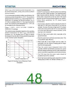
Thermal Considerations
For continuous operation, do not exceed absolute
maximum junction temperature. The maximum power
dissipation depends on the thermal resistance of the IC
package, PCB layout, rate of surrounding airflow, and
difference between junction and ambient temperature. The
maximum power dissipation can be calculated by the
following formula :
Under Voltage Lock Out (UVLO)
During normal operation, if the voltage at the VCC5 or
VCC12 pin drops below POR threshold, the AXGVR will
trigger UVLO. The UVLO protection forces all high side
MOSFETs and low side MOSFETs off by shutting down
internal PWM logic driver. A 3μs delay is used in UVLO
detection circuit to prevent false trigger.
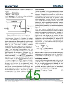
PD(MAX) = (TJ(MAX) − TA) / θJA
Copyright 2012 Richtek Technology Corporation. All rights reserved.
©
is a registered trademark of Richtek Technology Corporation.
DS8876A-02 October 2012
www.richtek.com
47

 RICHTEK [ RICHTEK TECHNOLOGY CORPORATION ]