RT8876A
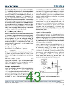
Considering the inductance tolerance, the resistor RX has
to be tuned on board by examining the transient voltage.
If the output voltage transient has an initial dip below the
minimum load line requirement with a slow recovery, RX
is chosen too small. Vice versa, if the resistance is too
large the output voltage transient has only a small initial
dip and the recovery becomes too fast, causing a ring
back to occur. Using current sense resistor in series with
the inductor can have better accuracy, but at the expense
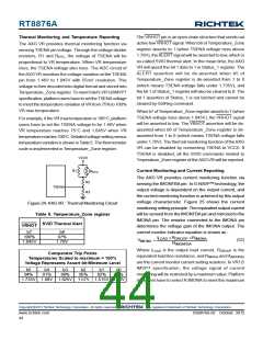
new operation state. When the AXG VR receives SetPS
command of PS2 operation mode, the AXGVR operates
as a single phase DCM controller and diode emulation
operation is activated. Therefore, an external driver which
supports tri-state shutdown is required for compatibility
with PS2 operation state.
If the AXG VR receives dynamic VID change command
(SetVID), the AXG VR will automatically enter PS0
operation mode. After VOUT,AXG reach target voltage, AXG
VR will stay at PS0 state and ignore former SetPS
command. Only by resending SetPS command after
SetVID command will the AXG VR be forced into PS2
operation state again.
of efficiency. Considering the equivalent inductance (LESL
)
of the current sense resistor, an RC filter is recommended.
The RC filter calculation method is similar to the above
mentioned inductorDCR sensing method.
No Load Offset (SVID & Platform)
Dynamic VID Enhancement
TheAXGVR features no load offset function which provides
the possibility of wide range positive offset of output voltage.
The no load offset function can be implemented through
the SVID interface or OFSA pin. Users can disable pin
offset function by simply connecting OFSA pin to GND.
The RT8876A will latch the OFSA status after POR. If pin
offset function is enabled, the OFSA pin voltage is more
than 0.6V before POR.
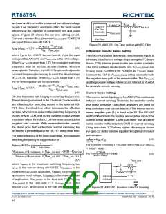
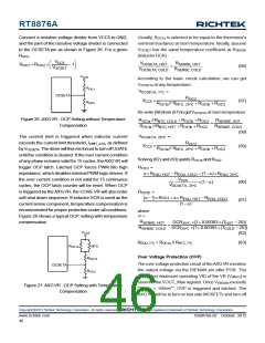
During a dynamic VID event, the charging (dynamic VID
up) or discharging (dynamic VID down) current causes
unwanted load-line effect which degrades the settling time
performance. TheDVIDApin can be used to compensate
the load-line effect, so that the output voltage can be settled
to the target value more quickly.
During a dynamic VID up event occurred, the RT8876A
sources out a current (IDVIDA) to DVIDA pin. The voltage
on DVIDA pin is added to DAC during DVID rising to
enhance the dynamic VID performance. Connecting a
capacitor in parallel with a resistor to DVIDA pin is
recommended. IDVIDA is 8μAduring a SetVID_Fast event.
If it is a SetVID_Slow event, IDVIDA automatically shrinks
to 2μA (if slow slew rate is 0.25x fast slew rate). This
function is null during a dynamic VID down event.
If then the output voltage is
V
= V
−I
×R
+ V
OUT
DAC
LOAD
DROOP PIN−OFS
(50)
+ V
SVID−OFS
The pin offset voltage is set by supplying a voltage into
OFSA pin. The linear range of offset pin voltage is from
0.9V to 1.83V. The pin offset voltage can be calculated as
below :
VPIN−OFSA = VOFSA − 1.2V
(51)
DAC
For example, supplying 1.3V at OFSA pin will achieve
100mV offset at the output. Connecting a filter capacitor
between the OFSA pin and GND is necessary.
Slew Rate
Control
I
DVIDA
DVID
Event
Operation Mode Transition
DVIDA
FBA
1/20
The RT8876Asupports operation mode transition function
at AXGVR for the SetPS command of Intel VR12/IMVP7
CPU. The default operation mode of theAXGVR is PS0,
which is CCM operation. Other operation mode includes
PS2 (single phaseDEM operation).After receiving SetPS
command, the AXG VR will immediately change to the
+
EA
-
Figure 23.DVIDCompensation Circuit
Copyright 2012 Richtek Technology Corporation. All rights reserved.
©
is a registered trademark of Richtek Technology Corporation.
DS8876A-02 October 2012
www.richtek.com
43

 RICHTEK [ RICHTEK TECHNOLOGY CORPORATION ]