RT8876A
voltage of IMONA at full load. Find RIMONA and RIMONFBA
based on :
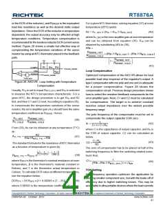
Quick Response
The AXGVR utilizes a quick response feature to support
heavy load current demand during instantaneous load
transient. The AXG VR monitors the current of the
IMONFBApin, and this current is mirrored to internal quick
response circuit. At steady state, this mirrored current
will not trigger a quick response. When the VOUT,AXG voltage
drops abruptly due to load apply transient, the mirrored
current into quick response circuit will also increase
instantaneously. When the mirrored current
instantaneously rises above 5μA, quick response will be
triggered.
V
RIMONA
IMONA(MAX)
=
(53)
RIMONFBA IMAX ×RDROOP
where VIMONA(MAX) is the maximum voltage at full load,
and IMAX is the full load current of VR.
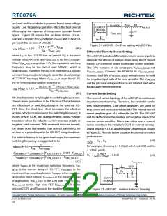
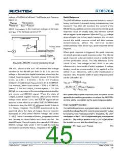
Current Mirror
FBA
+
-
V
CCAXG_SENSE
R
IMONFBA
IMONFBA
IMONA
I
Mirror
When quick response is triggered, the quick response
circuit will generate a quick response pulse. The internal
quick response pulse generation circuit is similar to the
on-time generation circuit. The only difference is the
QRSETA pin. The voltage at the QRSETA pin also
influences the pulse width of quick response. A voltage
divider circuit is recommended to be applied to the
QRSETA pin. Therefore, with a little modification of
equation (45), the pulse width of quick response pulse
can be calculated as :
R
IMONA
Figure 25. AXGVR : Current Monitoring Circuit
The ADC circuit of the AXG VR monitors the voltage
variation at the IMONA pin from 0V to 3.3V, and this
voltage is decoded into digital format and stored into the
Output_Current register. The ADC divides 3.3V into 255
levels, so LSB = 3.3V/255 = 12.941mV. Platform
designers should design VIMONA to be 3.3V at ICCMAXA.
For example, when load current = 50% x ICCMAXA,
VIMONA = 1.65V and Output_Current register = 7Fh. The
IMONApin is an output of the internal operational amplifier
and sends out IMONA signal. When the data of
Output_Current register reaches 255d (when IMONA
voltage rises above 3.3V), the ALERT signal will be
asserted to low, which is so-called SVID ICCMAXA alert.
In the mean time, the AXGVR will assert the bit 2 data to
1 in Status_1 register. The ALERT assertion will be de-
asserted when the data of Output_Current register
decreases to 242d (when IMONA voltage falls under
3.144V). The bit 2 assertion of Status_1 register is latched
and can only be cleared when two criteria are met : the
data of Output_Current register decreases to 242d (when
IMONA voltage falls under 3.144V) and the GetReg
command is sent to the Status_1 register of theAXGVR.
VQRSETA
tON, QR
=
× tON
1.2
20.33×10⁻¹² ×RTON × VQRSETA
=
(54)
VIN − VDAC, AXG
After generating a quick response pulse, the pulse is then
applied to the on-time generation circuit and theAXGVR's
on-time will be overridden by the quick response pulse.
Over Current Protection
The AXGVR compares a programmable current limit set
point to the voltage from the current sense amplifier output
for Over Current Protection (OCP). Therefore, the OCP
mechanism of the RT8876Aimplements per-phase current
protection. The voltage applied to the OCSETApin defines
the desired current limit threshold ILIMIT_AXG
:
VOCSETA = 48 x ILIMIT_AXG x RSENSE
(55)
Copyright 2012 Richtek Technology Corporation. All rights reserved.
©
is a registered trademark of Richtek Technology Corporation.
DS8876A-02 October 2012
www.richtek.com
45

 RICHTEK [ RICHTEK TECHNOLOGY CORPORATION ]