RT8876A
where TJ(MAX) is the maximum junction temperature, TA is
the ambient temperature, and θJA is the junction to ambient
thermal resistance.
Layout Considerations
Careful PC board layout is critical to achieve low switching
losses and clean, stable operation. The switching power
stage requires particular attention. If possible, mount all
of the power components on the top side of the board
with their ground terminals flushed against one another.
Follow these guidelines for PC board layout
considerations:
For recommended operating condition specifications, the
maximum junction temperature is 125°C. The junction to
ambient thermal resistance, θJA, is layout dependent. For
WQFN-56L 7x7 package, the thermal resistance, θJA, is
31°C/W on a standard JEDEC 51-7 four-layer thermal test
board. The maximum power dissipation at TA = 25°C can
be calculated by the following formula :
` Input ceramic capacitors must be placed to the drain of
high side FET and source of low side FET as close as
possible. The loop (The drain of high side FET to phase
node to the source of low side FET) is very critical due
to it is the main EMI source in Buck converter, so the
loop has to be minimized.
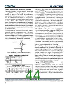
PD(MAX) = (125°C − 25°C) / (31°C/W) = 3.226W for
WQFN-56L 7x7 package
The maximum power dissipation depends on the operating
ambient temperature for fixed TJ(MAX) and thermal
resistance, θJA. The derating curve in Figure 26 allows
the designer to see the effect of rising ambient temperature
on the maximum power dissipation.
` Keep the high current paths short, especially at the
ground terminals.
` Keep the power traces and load connections short. This
is essential for high efficiency.
3.5
Four-Layers PCB
` When trade-offs in trace lengths must be made, it's
preferable to let the inductor charging path be longer
than the discharging path.
3.0
2.5
2.0
1.5
1.0
0.5
0.0
` Place the current sense component close to the
controller. ISENxP and ISENxNconnections for current
limit and voltage positioning must be made using Kelvin
sense connections to guarantee current sense accuracy.
` The PCB trace from the sense nodes should be
paralleled back to the controller.
0
25
50
75
100
125
` Route high speed switching nodes away from sensitive
Ambient Temperature (°C)
analog areas (COMP, FB, ISENxP, ISENxN, etc...)
Figure 26.Derating Curve of Maximum Power
Dissipation
Copyright 2012 Richtek Technology Corporation. All rights reserved.
©
is a registered trademark of Richtek Technology Corporation.
www.richtek.com
48
DS8876A-02 October 2012

 RICHTEK [ RICHTEK TECHNOLOGY CORPORATION ]