RT8859M
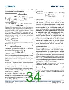
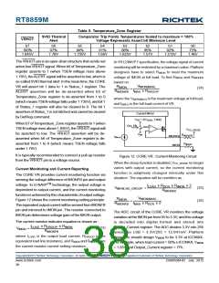
Table 5. Temperature_Zone Register
SVID Thermal
Comparator Trip Points Temperatures Scaled to maximum = 100%
Voltage Represents Assert bit Minimum Level
VRHOT
Alert
b7
b6
b5
b4
b3
b2
b1
b0
100%
1.845V
97%
1.79V
94%
1.735V
91%
1.68V
88%
1.625V
85%
1.57V
82%
1.515V
75%
1.46V
The VRHOT pin is an open-drain structure that sends out
active low VRHOT signal. When b6 of Temperature_Zone
register asserts to 1 (when TSEN voltage rises above
1.79V), theALERT signal will be asserted to low, which is
so-called SVIDthermal alert. In the mean time, the CORE
VR will assert bit 1 data to 1 in Status_1 register. The
ALERT assertion will be de-asserted when b5 of
Temperature_Zone register is de-asserted from 1 to 0
(which means TSENvoltage falls under 1.735V), and bit 1
of Status_1 register will also be cleared to 0. The bit 1
assertion of Status_1 is not latched and cannot be cleared
byGetReg command.
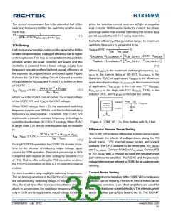
In VR12/IMVP7 specification, the voltage signal of current
monitoring will be restricted by a maximum value. Platform
designers have to select RIMON to meet the maximum
voltage of IMON at full load. To find RIMON and RIMONFB
based on :
V
RIMON
IMON(MAX)
(24)
=
RIMONFB IMAX x RDROOP
where the VIMON(MAX) is the maximum voltage at full load,
and I(MAX) is the full load current of VR.
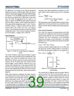
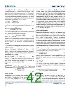
Current Mirror
V
FB
+ 2(V , Total)
ISEN
When b7 of Temperature_Zone register asserts to 1 (when
TSEN voltage rises above 1.845V), the VRHOT signal will
be asserted to low. The VRHOT assertion will be de-
asserted when b6 of Temperature_Zone register is de-
asserted from 1 to 0 (which means TSEN voltage falls
under 1.79V).
OLL EN
+
-
V
CC_SENSE
V
FB
R
IMONFB
IMONFB
IMON
I
Mirror
R
IMON
It is typically recommended to connect a pull-up resistor
from the VRHOT pin to a voltage source.
Figure 12. CORE VR : Current Monitoring Circuit
When the droop function is disabled, VCC_SENSE no longer
varies with output current, so the current monitoring
function is adaptively changed internally under this
situation. The equation will be rewritten as :
Current Monitoring and Current Reporting
The CORE VR provides current monitoring function via
sensing the voltage difference of IMONFB pin and output
voltage. In G-NAVPTM technology, the output voltage is
dependent to output current, and the current monitoring
function is achieved by this characteristic of output voltage.
Figure 12 shows the current monitoring setting principle.
The equivalent output current will be sensed from IMONFB
pin and mirrored to IMON pin. The resistor connected to
IMON pin determines voltage gain of the IMON output.
I
x R
x R
x 2
LOAD
DCR
IMON
V
=
(25)
(26)
IMON, NO_DROOP
R
IMONFB
V
RIMON
IMON(MAX)
=
RIMONFB IMAX x RDCR x 2
The ADC circuit of the CORE VR monitors the voltage
variation at the IMONpin from 0V to 3.3V, and this voltage
is decoded into digital format and stored into
Output_Current register. The ADC divides 3.3V into 255
levels, so LSB = 3.3V/255 = 12.941mV. Platform
designers should design VIMON to be 3.3V at ICCMAX.
For example, when load current = 50% x ICCMAX, VIMON
= 1.65V and Output_Current register = 7Fh.
The current monitor indicator equation is shown as :
I
x R
R
x R
LOAD
DROOP IMON
(23)
V
IMON
=
IMONFB
where ILOAD is the output load current, RDROOP is the
equivalent load line resistance, and RIMON and RIMONFB are
the current monitor current setting resistors.
Copyright 2012 Richtek Technology Corporation. All rights reserved.
©
is a registered trademark of Richtek Technology Corporation.
www.richtek.com
38
DS8859M-05 July 2012

 RICHTEK [ RICHTEK TECHNOLOGY CORPORATION ]