RT8859M
temperature variations of the sense resistor using anNTC
thermistor placed in the feedback path.
R1b =
RSENSE, HOT
x (R1a / /RNTC, HOT ) − (R1a / /RNTC, COLD
)
RSENSE, COLD
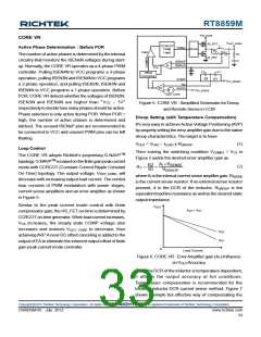
C2
C1
RSENSE, HOT
⎛
⎜
⎝
⎞
⎟
⎠
1−
RSENSE, COLD
(8)
R2
R1a
R1b
COMP
FB
V
CC_SENSE
R
NTC
-
EA
Droop Disable
RGND
V
+
SS_SENSE
The CORE VR's droop function can be enabled or disabled
with different connections of the QRSET pin. The
connection of the QRSET pin is usually a voltage divider
circuit which is described later in the Quick Response
section. Before POR, the RT8859M will source 80μA
current from the QRSET pin to the external voltage divider
to determine the voltage level while the RT8859M is still
not powered on. Before POR, if the voltage at the QRSET
pin is higher than VCC − 0.5V, the CORE VR will operate
in droop enabled mode. If the voltage is lower than
VCC − 1.8V, the CORE VR will operate without droop
function, which means at theDC level ofDAC voltage. For
example, a 5V voltage divided by two 1kΩ resistors
connected to the QRSET pin generates 2.54V (5V/2 +
80μA x 1kΩ/2) before POR and 2.5V (5V/2) after POR.
VDAC
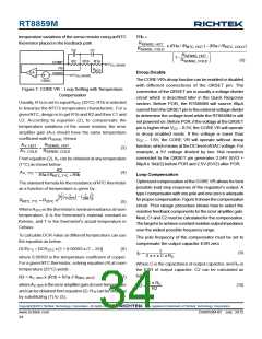
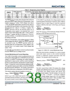
Figure 7. CORE VR : Loop Setting with Temperature
Compensation
Usually, R1a is set to equal RNTC (25°C). R1b is selected
to linearize the NTC's temperature characteristic. For a
given NTC, design is to get R1b and R2 and then C1 and
C2. According to equation (2), to compensate the
temperature variations of the sense resistor, the error
amplifier gain (AV) should have the same temperature
coefficient with RSENSE. Hence
A
R
SENSE, HOT
V, HOT
(3)
=
A
R
SENSE, COLD
V, COLD
From equation (2),AV can be obtained at any temperature
(T°C) as shown below :
R2
A
=
(4)
V, T°C
Loop Compensation
R1a // R
+ R1b
NTC, T°C
Optimized compensation of the CORE VR allows for best
possible load step response of the regulator's output. A
type-I compensator with one pole and one zero is adequate
for proper compensation. Figure 8 shows the compensation
circuit. Prior design procedure shows how to select the
resistive feedback components for the error amplifier gain.
Next, C1 and C2 must be calculated for the compensation.
The target is to achieve constant resistive output impedance
over the widest possible frequency range.
The standard formula for the resistance ofNTC thermistor
as a function of temperature is given by :
⎡
1
1
298
⎤
β
−
(
(
{
⎢
⎣
⎥
⎦
T+273
RNTC, T°C = R25°C
e
(5)
Where R25°C is the thermistor's nominal resistance at room
temperature, β is the thermistor's material constant in
Kelvins, and T is the thermistor's actual temperature in
Celsius.
To calculate DCR value at different temperature can use
the equation as below :
The pole frequency of the compensator must be set to
compensate the output capacitor ESR zero :
DCRT°C = DCR25°C x [1 + 0.00393 x (T − 25)]
(6)
1
(9)
fP =
2 x π x C x RC
where 0.00393 is the temperature coefficient of copper.
For a given NTC thermistor, solving equation (4) at room
temperature (25°C) yields :
Where C is the capacitance of output capacitor, and RC is
the ESR of output capacitor. C2 can be calculated as
follows :
R2 = AV, 25°C x (R1b + R1a // RNTC, 25°C
)
(7)
C x R
R2
C
whereAV, 25°C is the error amplifier gain at room temperature
and can be obtained from equation (2). R1b can be obtained
by substituting (7) to (3),
(10)
C2 =
Copyright 2012 Richtek Technology Corporation. All rights reserved.
©
is a registered trademark of Richtek Technology Corporation.
www.richtek.com
34
DS8859M-05 July 2012

 RICHTEK [ RICHTEK TECHNOLOGY CORPORATION ]