RT8859M
The IMON pin is an output of the internal operational
amplifier and sends out IMON signal. When the data of
Output_Current register reaches 255d (when IMONvoltage
rises above 3.3V), the ALERT signal will be asserted to
low, which is so-called SVID ICCMAX alert. In the mean
time, the CORE VR will assert the bit 2 data to 1 in
Status_1 register. TheALERT assertion will be de-asserted
when the data of Output_Current register decreases to
242d (when IMON voltage falls under 3.144V). The bit 2
assertion of Status_1 register is latched and can only be
cleared when two criteria are met : the data of
Output_Current register decreases to 242d (when IMON
voltage falls under 3.144V) and the GetReg command is
sent to the Status_1 register of the CORE VR.
Therefore, with a little modification of equation (12), the
pulse width of quick response pulse can be calculated
as :
VQRSET
tON, QR
=
x tON
1.2
20.33 x 10⁻¹² x RTON x VQRSET
=
(27)
VIN − VDAC
After generating a quick response pulse, the pulse is then
applied to the on-time generation circuit, and all the active
phases' on-times will be overridden by the quick response
pulse.
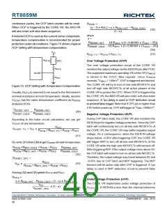
Over Current Protection
The CORE VR compares a programmable current limit
set point to the voltage from the current sense amplifier
output of each phase for Over Current Protection (OCP).
Therefore, the OCP mechanism of the RT8859M
implements per-phase current protections. The voltage
applied to the OCSET pin defines the desired current limit
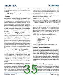
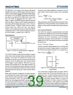
Quick Response
Current Mirror
VDAC
+
-
QR trigger
threshold, ILIMIT
:
R
IMONFB
IMONFB
I
Mirror
V
CC_SENSE
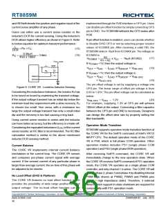
VOCSET = 48 x ILIMIT x RSENSE
(28)
Connect a resistive voltage divider from VCC toGND, and
the joint of the resistive voltage divider is connected to
the OCSET pin as shown in Figure 14. For a given ROC2
,
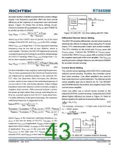
Figure 13. CORE VR : Quick Response Triggering
Circuit
V
⎛
⎞
CC
(29)
R
= R
x
−1
⎟
OC1
OC2
⎜
⎝
V
OCSET
⎠
The CORE VR utilizes a quick response feature to support
heavy load current demand during instantaneous load
transient. The CORE VR monitors the current of the
IMONFB pin, and this current is mirrored to internal quick
response circuit. At steady state, this mirrored current
will not trigger a quick response. When the VOUT, CORE
voltage drops abruptly due to load apply transient, the
mirrored current flowing into quick response circuit will
also increase instantaneously. When the mirrored current
instantaneously rises above 5μA, quick response will be
triggered.
V
CC
R
OC1
OCSET
R
OC2
Figure 14. OCP Setting without Temperature
Compensation
The current limit is triggered when per-phase inductor
current exceeds the current limit threshold, ILIMIT, as
defined by VOCSET. The driver will then be forced to turn off
UGATE until the condition is cleared. If the over current
condition of any phase remains valid for 15 cycles, the
CORE VR will trigger OCP latch. Latched OCP forces
PWM into high impedance, which disables internal PWM
logic drivers. If the over current condition is not valid for 15
When quick response is triggered, the quick response
circuit will generate a quick response pulse. The internal
quick response pulse generation circuit is similar to the
on-time generation circuit. The only difference is the
QRSET pin. The voltage at the QRSET pin also influences
the pulse width of quick response. Avoltage divider circuit
is recommended to be applied to the QRSET pin.
Copyright 2012 Richtek Technology Corporation. All rights reserved.
©
is a registered trademark of Richtek Technology Corporation.
DS8859M-05 July 2012
www.richtek.com
39

 RICHTEK [ RICHTEK TECHNOLOGY CORPORATION ]