RT8859M
continuous cycles, the OCP latch counter will be reset.
When OCP is triggered by the CORE VR, the AXG VR
will also enter soft shut down sequence.
ROC1b
=
(α −1) x ROC2 + α x REQU, HOT − REQU, COLD
(1− α)
(35)
where
α =
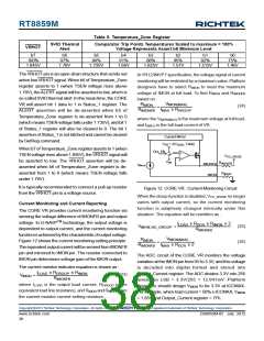
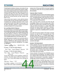
If inductorDCR is used as the current sense component,
temperature compensation is recommended for proper
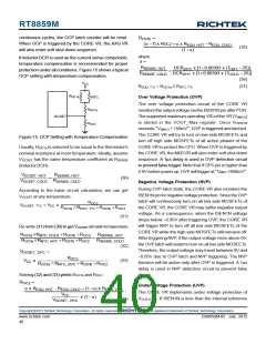
protection under all conditions. Figure 15 shows a typical
OCP setting with temperature compensation.
RSENSE, HOT
DCR25°C x [1+ 0.00393 x (THOT − 25)]
=
RSENSE, COLD DCR25°C x [1+ 0.00393 x (TCOLD − 25)]
(36)
V
CC
REQU, T°C = ROC1a // RNTC, T°C
(37)
R
OC1a
NTC
Over Voltage Protection (OVP)
The over voltage protection circuit of the CORE VR
monitors the output voltage via the ISEN1N pin after POR.
R
OC1b
The supported maximum operating VID of the VR (V(MAX)
)
OCSET
is stored in the VOUT_Max register. Once VISEN1N
exceeds “V(MAX) + 150mV”, OVP is triggered and latched.
The CORE VR will try to turn on low side MOSFETs and
turn off high side MOSFETs of all active phases of the
CORE VR to protect the CPU. When OVP is triggered by
the CORE VR, theAXGVR will also enter soft shut down
sequence. A 1μs delay is used in OVP detection circuit
to prevent false trigger. Note that if OFS pin is higher than
0.9V before power up, OVP will trigger at “VMAX +850mV”.
R
OC2
Figure 15. OCP Setting with Temperature Compensation
Usually, ROC1a is selected to be equal to the thermistor's
nominal resistance at room temperature. Ideally, assume
VOCSET has the same temperature coefficient as RSENSE
(InductorDCR) :
V
R
SENSE, HOT
OCSET, HOT
=
(30)
V
R
SENSE, COLD
OCSET, COLD
Negative Voltage Protection (NVP)
During OVP latch state, the CORE VR also monitors the
ISEN1N pin for negative voltage protection. Since the OVP
latch will continuously turn on all low side MOSFETs of
the CORE VR, the CORE VR may suffer negative output
voltage. As a consequence, when the ISEN1N voltage
drops below −0.05V after triggering OVP, the CORE VR
will trigger NVP to turn off all low side MOSFETs of the
CORE VR while the high side MOSFETs still remains off.
After triggeringNVP, if the output voltage rises above 0V,
the OVP latch will restart to turn on all low side MOSFETs.
Therefore, the output voltage may travel between 0V and
−0.05V due to OVP latch and NVP triggering. The NVP
function will be active only after OVP is triggered. A 1μs
delay is used in NVP detection circuit to prevent false
trigger.
According to the basic circuit calculation, we can get
VOCSET at any temperature:
R
OC2
V
= V
x
OCSET, T°C
CC
R
/ /R
+ R
+ R
OC1b OC2
OC1a
NTC, T°C
(31)
Re-write (31) from (30) to get VOCSET at room temperature
R
//R
+ R
+ R
+ R
+ R
R
SENSE, HOT
OC1a
NTC, COLD
OC1b
OC2
=
R
//R
R
SENSE, COLD
OC1a
NTC, HOT
OC1b
OC2
(32)
VOCSET, 25°C
VCC
=
ROC2
x
(33)
ROC1a / /RNTC, 25°C + ROC1b + ROC2
Solving (32) and (33) yields ROC1b and ROC2
ROC2
=
Under Voltage Protection (UVP)
α x REQU, HOT −REQU, COLD + (1− α) x REQU, 25°C
The CORE VR implements under voltage protection of
VOUT,CORE. If ISEN1N is less than the internal reference
VCC
VOCSET, 25°C
x (1− α)
(34)
Copyright 2012 Richtek Technology Corporation. All rights reserved.
©
is a registered trademark of Richtek Technology Corporation.
www.richtek.com
40
DS8859M-05 July 2012

 RICHTEK [ RICHTEK TECHNOLOGY CORPORATION ]