RT8859M
The zero of compensator has to be placed at half of the
switching frequency to filter the switching related noise.
when the inductor current reverses at light or negative
load currents. With reversed inductor current, the phase
goes high earlier than normal, extending the on-time by a
period equal to the HS-FET rising dead time.
Such that,
1
C1 =
(11)
R1b + R1a // R
× π× f
SW
(
)
NTC, 25°C
For better efficiency of the given load range, the maximum
switching frequency is suggested to be :
1
TON Setting
fS(MAX)(kHz) =
x
High frequency operation optimizes the application for the
smaller component size, trading off efficiency due to higher
switching losses. This may be acceptable in ultra portable
devices where the load currents are lower and the
controller is powered from a lower voltage supply. Low
frequency operation offers the best overall efficiency at
the expense of component size and board space. Figure
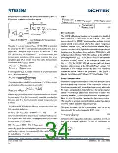
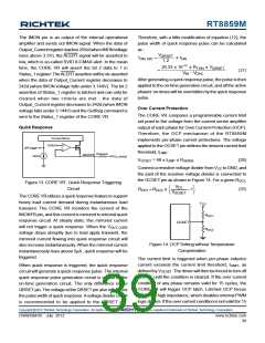
8 shows the On-Time setting Circuit. Connect a resistor
(RTON) between VIN,CORE and TONSET to set the on-time
of UGATE :
TON − THS−Delay
⎡
⎤
VDAC(MAX) +ILOAD(MAX) x RON_LS−FET + DCR − RDROOP
⎣
⎦
⎡
⎤
V
+ILOAD(MAX) x RON_LS−FET − RON_HS−FET
IN(MAX)
⎣
⎦
(14)
Where fS(MAX) is the maximum switching frequency, tHS-
is the turn-on delay of HS-FET, VDAC(MAX) is the
DELAY
Maximum VDAC of application, VIN(MAX) is the Maximum
application Input voltage, ILOAD(MAX) is the maximum load
of application, RON_LS-FET is the Low side FET RDS(ON)
,
24.4 x 10⁻¹² x R
TON
(12)
t
(V
DAC
< 1.2V) =
RON_HS-FET is the High side FET RDS(ON), DCRL is the
inductor DCR, and RDROOP is the load line setting.
ON
V
− V
DAC
IN
where tON is the UGATE turn on period, VIN is Input voltage
of the CORE VR, and VDAC is the DAC voltage.
R
R1
C1
TON
TONSET
VDAC
V
IN, CORE
CCRCOT
On-Time
Computer
When VDAC is larger than 1.2V, the equivalent switching
frequency may be over 500kHz, and this too fast switching
frequency is unacceptable. Therefore, the CORE VR
implements a pseudo constant frequency technology to
avoid this disadvantage of CCRCOT topology. When VDAC
is larger than 1.2V, the on-time equation will be modified
to :
On-Time
Figure 8. CORE VR : On-Time Setting with RC Filter
Differential Remote Sense Setting
20.33 x 10⁻¹² x R
x V
DAC
The CORE VR includes differential, remote-sense inputs
to eliminate the effects of voltage drops along the PC
board traces, CPU internal power routes and socket
contacts. The CPU contains on-die sense pins, VCC_SENSE
and VSS_SENSE. Connect RGNDto VSS_SENSE. Connect FB
to VCC_SENSE with a resistor to build the negative input
path of the error amplifier. The VDAC and the precision
voltage reference are referred to RGNDfor accurate remote
sensing.
TON
t
(V
DAC
≥ 1.2V) =
ON
V
IN
− V
DAC
(13)
During PS2/PS3 operation, the CORE VR shrinks its on-
time for the purpose of reducing output voltage ripple
caused byDCM operation. The shrink percentage is 15%
compared with original on-time setting by equation (12)
or (13). That is, after setting the PS0 operation on-time,
the PS2/PS3 operation on-time is 0.85 times the original
on-time.
Current Sense Setting
On-time translates only roughly to switching frequencies.
The on-times guaranteed in the Electrical Characteristics
are influenced by switching delays in external HS-FET.
Also, the dead-time effect increases the effective on-time,
which in turn reduces the switching frequency. It occurs
only in CCM and during dynamic output voltage transitions
The current sense topology of the CORE VR is continuous
inductor current sensing. Therefore, the controller can be
less noise sensitive. Low offset amplifiers are used for
loop control and over current detection. The internal current
sense amplifier gain (Ai) is fixed to be 10. The ISENxP
Copyright 2012 Richtek Technology Corporation. All rights reserved.
©
is a registered trademark of Richtek Technology Corporation.
DS8859M-05 July 2012
www.richtek.com
35

 RICHTEK [ RICHTEK TECHNOLOGY CORPORATION ]