RT6343
ceramic capacitor with X7R is recommended, and the
capacitor should have a 6.3 V or higher voltage rating.
External Bootstrap Resistor (Option)
The gate driver of an internal high-side MOSFET, utilized
as a high-side switch, is optimized for turning on the
switch. The gate driver is not only fast enough for reducing
switching power loss, but also slow enough for minimizing
EMI. The EMI issue is worse when the switch is turned
on rapidly due to induced high di/dt noises. When the
high-side MOSFET is turned off, the SW node will be
discharged relatively slow by the inductor current because
the presence of the dead time when both the high-side
MOSFET and low-side freewheel diode are turned off.
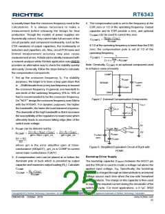
External Bootstrap Diode
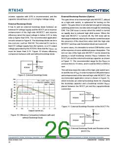
It has to add an external bootstrap diode between an
external 5V voltage supply and the BOOT pin to improve
enhancement of the high-side MOSFET and improve
efficiency when the input voltage is below 5.5V or duty
ratio is higher than 65%. The recommended application
circuit is shown in Figure 9. The bootstrap diode can be a
low-cost one, such as 1N4148. The external 5V can be a
fixed 5V voltage supply from the system, or a 5V output
voltage generated by the RT6343.Note that the VBOOT−SW
must be lower than 5.5V. Figure 10 shows efficiency
comparison between with and without bootstrap diode.
5V
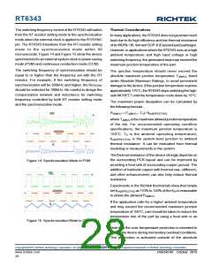
In some cases, it is desirable to reduce EMI further, even
at the expense of some additional power dissipation. The
turn-on rate of the high-side MOSFET can be slowed by
placing a small bootstrap resistor RBOOT between the
BOOT pin and the external bootstrap capacitor as shown
in Figure 11. The recommended range for the RBOOT is
several ohms to 10 ohms, and it could be 0402 or 0603 in
size.
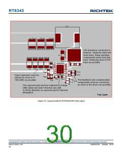
D
BOOT
BOOT
RT6343
SW
C
0.1µF
BOOT
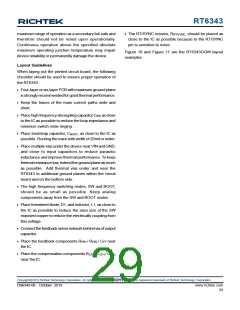
This will slow down the rates of the high-side switch turn-
on and the rise of VSW. In order to improve EMI performance
and enhancement of the internal high-side MOSFET, the
recommended application circuit is shown in Figure 12,
which includes an external bootstrap diode for charging
the bootstrap capacitor and a bootstrap resistor RBOOT
placed between the BOOT pin and the capacitor/diode
connection.
Figure 9. External Bootstrap Diode
100
98
96
94
92
90
88
86
84
82
80
VIN = 4.5V, VOUT = 3.3V
L = VCHA075D-100MS6, 10μH
f
= 300kHz
SW
With Bootstrap Diod
R
BOOT
Without Bootstrap Diode
BOOT
SW
C
BOOT
RT6343
Figure 11. External Bootstrap Resistor at the BOOT Pin
0
0.5
1
1.5
2
2.5
3
3.5
5V
Output Current (A)
D
BOOT
Figure 10. Efficiency Comparison between with and
without BootstrapDiode
R
BOOT
BOOT
SW
C
RT6343
BOOT
Figure 12. External Bootstrap Diode and Resistor at the
BOOT Pin
Copyright 2019 Richtek Technology Corporation. All rights reserved.
©
is a registered trademark of Richtek Technology Corporation.
www.richtek.com
26
DS6343-00 October 2019

 RICHTEK [ RICHTEK TECHNOLOGY CORPORATION ]