RT6343
is usually lower than the crossover frequency used in the
calculations. It is always necessary to make a
measurement before releasing the design for final
production. Though the models of power supplies are
theoretically correct, they cannot take full account of the
circuit parasitic and component nonlinearity, such as the
ESR variations of output capacitors, the nonlinearity of
inductors and capacitors, etc.Also, circuit PCB noise and
limited measurement accuracy may also cause
measurement errors.ABode plot is ideally measured with
a network analyzer while Richtek application noteAN038
provides an alternative way to check the stability quickly
and easily. Generally, follow the steps below to calculate
the compensation components :
4. The compensation pole is set to the frequency at the
ESR zero or 1/2 of the operating frequency. Output
capacitor and its ESR provide a zero, and optional
CCOMP2 can be used to cancel this zero.
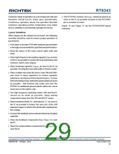
R
C
COMP
ESR
R
OUT
C
COMP2
=
If 1/2 of the operating frequency is lower than the ESR
zero, the compensation pole is set at 1/2 of the
operating frequency.
1
C
COMP2
=
fsw
2
2
R
COMP
Note: Generally, CCOMP2 is an optional component used
to enhance noise immunity.
COMP
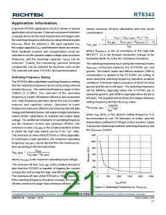
1. Set up the crossover frequency, fC. For stability
purposes, the target is to have a loop gain slope that
is −20dB/decade from a very low frequency to beyond
the crossover frequency. In general, one-twentieth to
one-tenth of the switching frequency (5% to 10% of
fsw) is recommended to be the crossover frequency.
Do “NOT” design the crossover frequency over 80kHz
with the RT6343. For dynamic purposes, the higher
the bandwidth, the faster the load transient response.
The downside of the high bandwidth is that it increases
the susceptibility of the regulators to board noise which
ultimately leads to excessive falling edge jitter of the
switch node voltage.
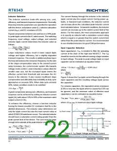
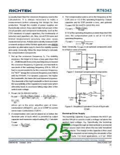
R
COMP
C
COMP2
RT6343
(option)
C
COMP
GND
Figure 7. External Compensation Components
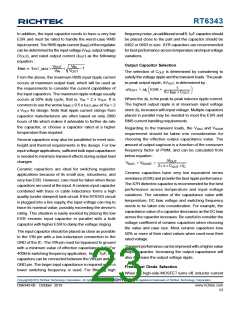
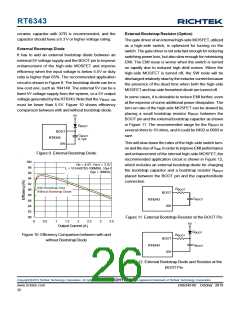
V
OUT
R
ESR
gm_cs
R
L
C
OUT
R1
R2
V
FB
-
V
2. RCOMP can be determi ned by :
COMP
EA
+
V
REF
2 fC VOUT COUT
gm VREF gm_cs
2 fC COUT
gmgm_cs
RCOMP
=
=
R
COMP
C
COMP2
(option)
C
R1 + R2
R2
COMP
where gm is the error amplifier gain of trans-
conductance (440μA/V) ; gm_cs is COMP to current
sense trans-conductance (12A/V)
Figure 8. Simplified Equivalent Circuit of Buck with
PCMC
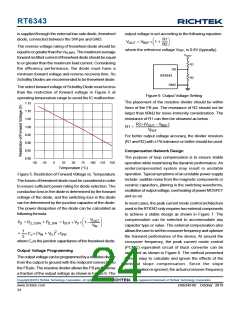
Bootstrap Driver Supply
3. A compensation zero can be placed at or before the
dominant pole of buck which is provided by output
capacitor and maximum output loading (RL). Calculate
The bootstrap capacitor (CBOOT) between the BOOT pin
and the SW pin is used to create a voltage rail above the
applied input voltage, VIN. Specifically, the bootstrap
capacitor is charged through an internal diode to an internal
voltage source each time when the low-side freewheel
diode conducts. The charge on this capacitor is then used
to supply the required current during the remainder of the
switching cycle. For most applications, a 0.1μF, 0603
CCOMP
:
R C
L
OUT
C
COMP
=
R
COMP
Copyright 2019 Richtek Technology Corporation. All rights reserved.
©
is a registered trademark of Richtek Technology Corporation.
DS6343-00 October 2019
www.richtek.com
25

 RICHTEK [ RICHTEK TECHNOLOGY CORPORATION ]