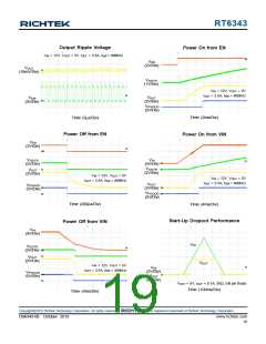
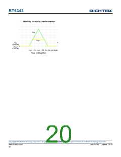
RT6343
In addition, the input capacitor needs to have a very low
ESR and must be rated to handle the worst-case RMS
input current. The RMS ripple current (IRMS) of the regulator
can be determined by the input voltage (VIN), output voltage
(VOUT), and rated output current (IOUT) as the following
equation :
frequency noise, an additional small 0.1μF capacitor should
be placed close to the part and the capacitor should be
0402 or 0603 in size. X7R capacitors are recommended
for best performance across temperature and input voltage
variations.
Output Capacitor Selection
V
V
V
IN
V
OUT
OUT
I
I
1
RMS
OUT_MAX
IN
The selection of COUT is determined by considering to
satisfy the voltage ripple and the transient loads. The peak-
to-peak output ripple, ΔVOUT, is determined by :
From the above, the maximum RMS input ripple current
occurs at maximum output load, which will be used as
the requirements to consider the current capabilities of
the input capacitors. The maximum ripple voltage usually
occurs at 50% duty cycle, that is, VIN = 2 x VOUT. It is
common to use the worse IRMS ≅ 0.5 x IOUT_MAX at VIN = 2
x VOUT for design. Note that ripple current ratings from
capacitor manufacturers are often based on only 2000
hours of life which makes it advisable to further de-rate
the capacitor, or choose a capacitor rated at a higher
temperature than required.
1
VOUT = IL ESR +
8fSW COUT
Where the ΔIL is the peak-to-peak inductor ripple current.
The highest output ripple is at maximum input voltage
since ΔIL increases with input voltage. Multiple capacitors
placed in parallel may be needed to meet the ESR and
RMS current handling requirements.
Regarding to the transient loads, the VSAG and VSOAR
requirement should be taken into consideration for
choosing the effective output capacitance value. The
amount of output sag/soar is a function of the crossover
frequency factor at PWM, and can be calculated from
Several capacitors may also be paralleled to meet size,
height and thermal requirements in the design. For low
input voltage applications, sufficient bulk input capacitance
is needed to minimize transient effects during output load
changes.
below equation :
IOUT
2 COUT fC
VSAG = VSOAR
=
Ceramic capacitors are ideal for switching regulator
applications because of its small size, robustness, and
very low ESR. However, care must be taken when these
capacitors are used at the input.Aceramic input capacitor
combined with trace or cable inductance forms a high
quality (under damped) tank circuit. If the RT6343 circuit
is plugged into a live supply, the input voltage can ring to
twice its nominal value, possibly exceeding the device's
rating. This situation is easily avoided by placing the low
ESR ceramic input capacitor in parallel with a bulk
capacitor with higher ESR to damp the voltage ringing.
Ceramic capacitors have very low equivalent series
resistance (ESR) and provide the best ripple performance.
The X7R dielectric capacitor is recommended for the best
performance across temperature and input voltage
variations. The variation of the capacitance value with
temperature, DC bias voltage and switching frequency
needs to be taken into consideration. For example, the
capacitance value of a capacitor decreases as theDC bias
across the capacitor increases. Be careful to consider the
voltage coefficient of ceramic capacitors when choosing
the value and case size. Most ceramic capacitors lose
50% or more of their rated values when used near their
rated voltage.
The input capacitor should be placed as close as possible
to the VIN pin with a low inductance connection to the
GND of the IC. The VIN pin must be bypassed to ground
with a minimum value of effective capacitance 3μF. For
400kHz switching frequency application, two 4.7μF, X7R
capacitors can be connected between the VINpin and the
GNDpin. The larger input capacitance is required when a
lower switching frequency is used. For filtering high
Transient performance can be improved with a higher value
output capacitor. Increasing the output capacitance will
also decrease the output voltage ripple.
Freewheel Diode Selection
When the high-side MOSFET turns off, inductor current
is a registered trademark of Richtek Technology Corporation.
Copyright 2019 Richtek Technology Corporation. All rights reserved.
©
DS6343-00 October 2019
www.richtek.com
23

 RICHTEK [ RICHTEK TECHNOLOGY CORPORATION ]