RT6343
is supplied through the external low-side diode, freewheel
diode, connected between the SW pin and GND.
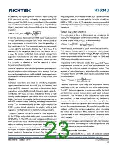
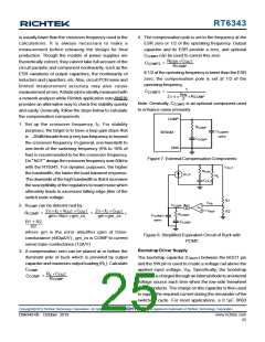
output voltage is set according to the following equation :
R1
R2
V
= V
1 +
OUT
REF
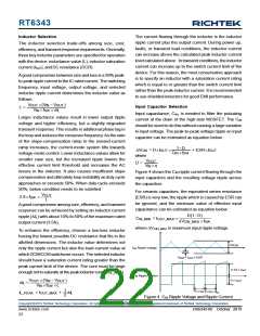
The reverse voltage rating of freewheel diode should be
equal to or greater than the VIN_MAX. The maximum average
forward rectified current of freewheel diode should be equal
to or greater than the maximum load current. Considering
the efficiency performance, the diode must have a
minimum forward voltage and reverse recovery time. So
SchottkyDiodes are recommended to be freewheel diode.
where the reference voltage VREF, is 0.8V (typically).
V
OUT
R1
FB
RT6343
R2
GND
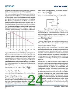
The select forward voltage of SchottkyDiode must be less
than the restriction of forward voltage in Figure 5 at
operating temperature range to avoid the IC malfunction.
1.15
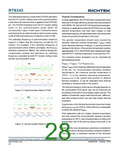
Figure 6. Output Voltage Setting
The placement of the resistive divider should be within
5mm of the FB pin. The resistance of R2 should not be
larger than 80kΩ for noise immunity consideration. The
resistance of R1 can then be obtained as below :
1.10
1.05
1.00
0.95
0.90
0.85
0.80
R2(VOUT VREF
)
R1 =
VREF
For better output voltage accuracy, the divider resistors
(R1 and R2) with 1% tolerance or better should be used.
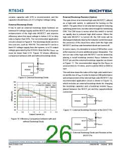
Compensation Network Design
The purpose of loop compensation is to ensure stable
operation while maximizing the dynamic performance.An
undercompensated system may result in unstable
operation. Typical symptoms of an unstable power supply
include: audible noise from the magnetic components or
ceramic capacitors, jittering in the switching waveforms,
oscillation of output voltage, overheating of power MOSFET
and so on.
-50
-25
0
25
50
75
100 125 150
Temperature (°C)
Figure 5. Restriction of Forward Voltage vs. Temperature
The losses of freewheel diode must be considered in order
to ensure sufficient power rating for diode selection. The
conduction loss in the diode is determined by the forward
voltage of the diode, and the switching loss in the diode
can be determined by the junction capacitor of the diode.
The power dissipation of the diode can be calculated as
following formula
In most cases, the peak current mode control architecture
used in the RT6343 only requires two external components
to achieve a stable design as shown in Figure 7. The
compensation can be selected to accommodate any
capacitor type or value. The external compensation also
allows the user to set the crossover frequency and optimize
the transient performance of the device. At around the
crossover frequency, the peak current mode control
(PCMC) equivalent circuit of Buck converter can be
simplified as shown in Figure 8. The method presented
here is easy to calculate and ignore the effects of the
internal slope compensation. Since the slope
compensation is ignored, the actual crossover frequency
VOUT
V
PD = PD_CON + PD_SW = IOUT V 1
D
IN
1
+
C V + VD 2 fSW
J IN
2
where CJ is the junction capacitance of the freewheel diode.
Output Voltage Programming
The output voltage can be programmed by a resistive divider
from the output to ground with the midpoint connected to
the FB pin. The resistive divider allows the FB pin to sense
a fraction of the output voltage as shown in Figure 6. The
Copyright 2019 Richtek Technology Corporation. All rights reserved.
©
is a registered trademark of Richtek Technology Corporation.
www.richtek.com
24
DS6343-00 October 2019

 RICHTEK [ RICHTEK TECHNOLOGY CORPORATION ]