RT6343
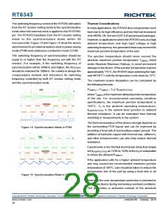
The switching frequency control of the RT6343 will switch
from the RT resistor setting mode to the synchronization
mode when the external clock is applied to the RT/SYNC
pin. The RT6343 transitions from the RT resistor setting
mode to the synchronization mode within 60
microseconds. Figure 14 and Figure 15 show the device
synchronized to an external system clock in power saving
mode (PSM) and continuous conduction mode (CCM).
Thermal Considerations
In many applications, the RT6343 does not generate much
heat due to its high efficiency and low thermal resistance
of its WDFN-10L4x4 and SOP-8 (Exposed pad) packages.
However, in applications which the RT6343 runs at a high
ambient temperature and high input voltage or high
switching frequency, the generated heat may exceed the
maximum junction temperature of the part.
The switching frequency of synchronization should be
equal to or higher than the frequency set with the RT
resistor. For example, if the switching frequency of
synchronization will be 300kHz and higher, the RRT/SYNC
should be selected for 300kHz. Be careful to design the
compensation network and inductance for switching
frequency controlled by both RT resistor setting mode
and the synchronization mode.
The junction temperature should never exceed the
absolute maximum junction temperature TJ(MAX), listed
under Absolute Maximum Ratings, to avoid permanent
damage to the device. If the junction temperature reaches
approximately 175°C, the RT6343 stops switching the high-
side MOSFET until the temperature cools down by 15°C.
The maximum power dissipation can be calculated by
the following formula :
PD(MAX) = (TJ(MAX) − TA) / θJA(EFFECTIVE)
where TJ(MAX) is the maximum allowed junction temperature
of the die. For recommended operating condition
specifications, the maximum junction temperature is
150°C. TA is the ambient operating temperature,
θJA(EFFECTIVE) is the system-level junction to ambient
thermal resistance. It can be estimated from thermal
modeling or measurements in the system.
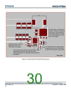
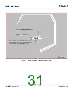
The thermal resistance of the device strongly depends on
the surrounding PCB layout and can be improved by
providing a heat sink of surrounding copper ground. The
addition of backside copper with thermal vias, stiffeners,
and other enhancements can also help reduce thermal
resistance.
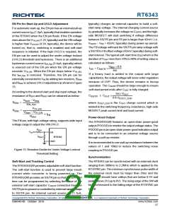
Figure 14. Synchronization Mode in PSM
Experiments in the Richtek thermal lab show that simply
set θJA(EFFECTIVE) as 110% to 120% of the θJA is reasonable
to obtain the allowed PD(MAX)
.
If the application calls for a higher ambient temperature
and may exceed the recommended maximum junction
temperature of 150°C, care should be taken to reduce the
temperature rise of the part by using a heat sink or air
flow.
Figure 15. Synchronization Mode in CCM
Note that the over-temperature protection is intended to
protect the device during momentary overload conditions.
The protection is activated outside of the absolute
Copyright 2019 Richtek Technology Corporation. All rights reserved.
©
is a registered trademark of Richtek Technology Corporation.
www.richtek.com
28
DS6343-00 October 2019

 RICHTEK [ RICHTEK TECHNOLOGY CORPORATION ]