RT6343
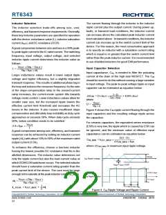
Inductor Selection
The current flowing through the inductor is the inductor
ripple current plus the output current. During power up,
faults, or transient load conditions, the inductor current
can increase above the calculated peak inductor current
level calculated above . In transient conditions, the inductor
current can increase up to the switch current limit of the
device. For this reason, the most conservative approach
is to specify an inductor with a saturation current rating
which is equal to or greater than the switch current limit
rather than the peak inductor current. It is recommended
to use shielded inductors for good EMI performance.
The inductor selection trade-offs among size, cost,
efficiency, and transient response requirements.Generally,
three key inductor parameters are specified for operation
with the device: inductance value (L), inductor saturation
current (ISAT), andDC resistance (DCR).
Agood compromise between size and loss is a 30% peak-
to-peak ripple current to the IC rated current. The switching
frequency, input voltage, output voltage, and selected
inductor ripple current determines the inductor value as
follows :
V
(V V
)
OUT
IN
OUT
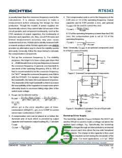
Input Capacitor Selection
L =
V f
I
IN SW
L
Input capacitance, CIN, is needed to filter the pulsating
current at the drain of the high-side MOSFET. The CIN
should be sized to do this without causing a large variation
in input voltage. The peak-to-peak voltage ripple on input
capacitor can be estimated as equation below :
Larger inductance values result in lower output ripple
voltage and higher efficiency, but a slightly degraded
transient response. This results in additional phase lag in
the loop and reduces the crossover frequency.As the ratio
of the slope-compensation ramp to the sensed-current
ramp increases, the current-mode system tilts towards
voltage-mode control. Lower inductance values allow for
smaller case size, but the increased ripple lowers the
effective current limit threshold and increases the AC
losses in the inductor. It also causes insufficient slope
compensation and ultimately loop instability as duty cycle
approaches or exceeds 50%. When duty cycle exceeds
50%, below condition needs to be satisfied :
1D
IN SW
V
where
D =
= DI
+ ESRI
OUT
CIN
OUT
C
f
V
OUT
V
IN
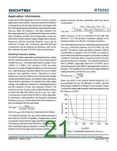
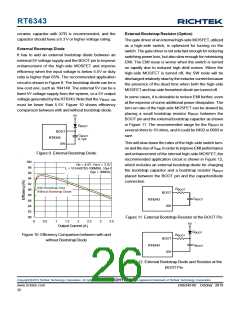
Figure 4 shows the CIN ripple current flowing through the
input capacitors and the resulting voltage ripple across
the capacitors.
For ceramic capacitors, the equivalent series resistance
(ESR) is very low, the ripple which is caused by ESR can
be ignored, and the minimum value of effective input
capacitance can be estimated as equation below :
D 1D
VOUT
L
2.9fSW
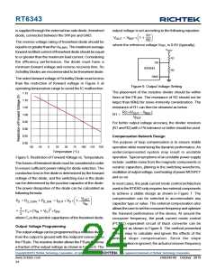
Agood compromise among size, efficiency, and transient
response can be achieved by setting an inductor current
ripple (ΔIL) with about 10% to 50% of the maximum rated
output current (3.5A).
C
IN_MIN
= I
OUT_MAX
V
f
CIN_MAX SW
where ΔVCIN_MAX is maximum input ripple voltage.
To enhance the efficiency, choose a low-loss inductor
having the lowest possible DC resistance that fits in the
allotted dimensions. The inductor value determines not
only the ripple current but also the load-current value at
whichDCM/CCM switchover occurs. The selected inductor
should have a saturation current rating greater than the
peak current limit of the device. The core must be large
enough not to saturate at the peak inductor current (IL_PEAK) :
V
CIN
C
Ripple Voltage
IN
V
ESR
= I
OUT
x ESR
(1-D) x I
OUT
C
Ripple Current
IN
D x I
OUT
V
OUT
(V V
OUT
)
IN
I =
L
V f
L
IN SW
1
2
D x tSW
(1-D) x tSW
IL_PEAK = IOUT_MAX
+
IL
Figure 4. CIN Ripple Voltage and Ripple Current
Copyright 2019 Richtek Technology Corporation. All rights reserved.
©
is a registered trademark of Richtek Technology Corporation.
www.richtek.com
22
DS6343-00 October 2019

 RICHTEK [ RICHTEK TECHNOLOGY CORPORATION ]