RT6343
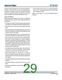
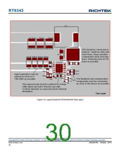
L1
COUT2
COUT3
COUT1
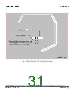
SW should be connected to
inductor / diode by wide and
short trace. Keep sensitive
components away from this
trace. Reducing area of SW
trace as possible.
D1
CIN5
CIN1 CIN2
CIN3
CIN4
REN1
REN2
CCP2
CCP1
Input capacitors must be
placed as close to IC
VIN-GND as possible.
RCP1
RRT
RFB2
RFB1
CFF
CSS
The feedback and compensation
components must be connected
as close to the device as possible.
The exposed pad must be soldered to a large
GND plane and add 6 thermal vias with
0.25mm diameter on exposed pad for thermal
dissipation.
Top Layer
Figure 16. LayoutGuide for RT6343GQW (Top Layer)
Copyright 2019 Richtek Technology Corporation. All rights reserved.
is a registered trademark of Richtek Technology Corporation.
©
www.richtek.com
30
DS6343-00 October 2019

 RICHTEK [ RICHTEK TECHNOLOGY CORPORATION ]