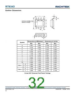
RT6343
maximum range of operation as a secondary fail-safe and
therefore should not be relied upon operationally.
Continuous operation above the specified absolute
maximum operating junction temperature may impair
device reliability or permanently damage the device.
The RT/SYNC resistor, RRT/SYNC, should be placed as
close to the IC as possible because to the RT/SYNC
pin is sensitive to noise.
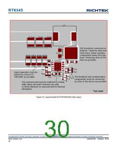
Figure 16 and Figure 17 are the RT6343GQW layout
examples.
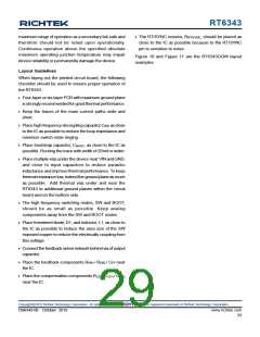
Layout Guidelines
When laying out the printed circuit board, the following
checklist should be used to ensure proper operation of
the RT6343 :
Four-layer or six-layer PCB with maximum ground plane
is strongly recommended for good thermal performance.
Keep the traces of the main current paths wide and
short.
Place high frequency decoupling capacitor CIN5 as close
to the IC as possible to reduce the loop impedance and
minimize switch node ringing.
Place bootstrap capacitor, CBOOT, as close to the IC as
possible. Routing the trace with width of 20mil or wider.
Place multiple vias under the device near VINandGND,
and close to input capacitors to reduce parasitic
inductance and improve thermal performance. To keep
thermal resistance low, extend the ground plane as much
as possible. Add thermal vias under and near the
RT6343 to additional ground planes within the circuit
board and on the bottom side.
The high frequency switching nodes, SW and BOOT,
should be as small as possible. Keep analog
components away from the SW and BOOT nodes.
Place freewheel diode,D1, and inductor, L1, as close to
the IC as possible to reduce the area size of the SW
exposed copper to reduce the electrically coupling from
this voltage.
Connect the feedback sense network behind via of output
capacitor.
Place the feedback components RFB1 / RFB2 / CFF near
the IC.
Place the compensation components RCP1 / CCP1 / CCP2
near the IC.
Copyright 2019 Richtek Technology Corporation. All rights reserved.
©
is a registered trademark of Richtek Technology Corporation.
DS6343-00 October 2019
www.richtek.com
29

 RICHTEK [ RICHTEK TECHNOLOGY CORPORATION ]