RT6263A/B
to the variation of junction temperature is dominated by
the ambient temperature, the T'J at 35°C ambient
temperature can be pre-estimated as
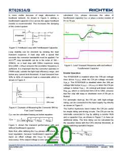
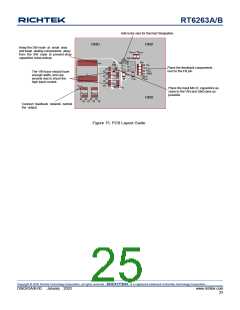
Layout Considerations
Follow the PCB layout guidelines below for optimal
performance of the device.
T' = 110.9C + 35C 25C = 120.9C
J
Keep the high-current paths short, especially at the
ground terminals. This practice is essential for stable
and jitter-free operation. The high current path
comprising of input capacitor, high-side FET,
inductor, and the output capacitor should be as short
as possible. This practice is essential for high
efficiency.
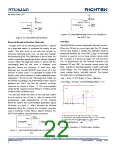
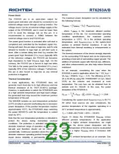
According to Figure 14, the increasing RDS(ON) can be
found as
R
= 90.5m (at 120.9C) 88m 110.9C
DS ON _H
= 2.5m
R
= 44.7m at 120.9C 43.7m 110.9C
DS ON _L
= 1m
Place the input MLCC capacitors as close to the VIN
and GND pins as possible. The major MLCC
capacitors should be placed on the same layer as
the RT6263A/B.
The external power dissipation caused by the
increasing RDS(ON) at higher temperature can be
calculated as
SW node is with high frequency voltage swing and
should be kept at small area. Keep analog
components away from the SW node to prevent
stray capacitive noise pickup.
3.3
12
3.3
12
2
2
P
= 3A
2.5m + 3A 1
1m
D,RDS ON
= 0.013W
As a result, the new power dissipation is 1.263W due to
the variation of RDS(ON). Therefore, the estimated new
junction temperature is
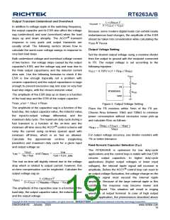
Connect feedback network behind the output
capacitors. Place the feedback components next to
the FB pin.
For better thermal performance, to design a wide
and thick plane for GND pin or to add a lot of vias to
GND plane.
T'J = 1.263W68.7C/W + 35C = 121.77C
If the application requires a higher ambient temperature
and may exceed the recommended maximum junction
temperature of 125°C, care should be taken to reduce
the temperature rise of the part by using a heat sink or
air flow.
An example of PCB layout guide is shown in Figure 15.
Resistance vs. Temperature
250
200
150
RDS(ON)_H
RDS(ON)_L
100
50
0
-50
-25
0
25
50
75
100
125
Temperature (°C)
Figure 14. RT6263A/B RDS(ON) vs. Temperature
Copyright © 2020 Richtek Technology Corporation. All rights reserved.
is a registered trademark of Richtek Technology Corporation.
www.richtek.com
24
DS6263A/B-00 January 2020

 RICHTEK [ RICHTEK TECHNOLOGY CORPORATION ]