RT6263A/B
2
Output Transient Undershoot and Overshoot
L(IOUT
)
VSOAR
=
2COUT VOUT
In addition to voltage ripple at the switching frequency,
the output capacitor and its ESR also affect the voltage
sag (undershoot) and soar (overshoot) when the load
steps up and down abruptly. The ACOT® transient
response is very quick and output transients are
usually small. The following section shows how to
calculate the worst-case voltage swings in response to
very fast load steps.
Because some modern digital loads can exhibit nearly
instantaneous load changes, the amplitude of the ESR
should be taken into consideration while calculating the
VSAG & VSOAR
.
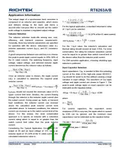
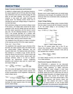
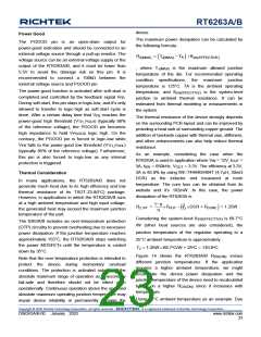
Output Voltage Setting
Set the desired output voltage using a resistive divider
from the output to ground with the midpoint connected
to FB. The output voltage is set according to the
following equation :
Both undershoot voltage and overshoot voltage consist
of two factors : the voltage steps caused by the output
capacitor's ESR, and the voltage sag and soar due to
the finite output capacitance and the inductor current
slew rate. Use the following formulas to check if the
ESR is low enough (typically not a problem with
ceramic capacitors) and the output capacitance is large
enough to prevent excessive sag and soar on very fast
load step edges, with the chosen inductor value.
VOUT = 0.765V x (1 + RFB1 / RFB2
)
V
OUT
R
R
FB1
FB2
FB
RT6263A/B
The amplitude of the ESR step up or down is a function
of the load step and the ESR of the output capacitor :
GND
VESR _STEP = IOUT x RESR
Figure 2. Output Voltage Setting
The amplitude of the capacitive sag is a function of the
load step, the output capacitor value, the inductor value,
the input-to-output voltage differential, and the
maximum duty cycle. The maximum duty cycle during a
fast transient is a function of the on-time and the
minimum off-time since the ACOT® control scheme will
ramp the current using on-times spaced apart with
minimum off-times, which is as fast as allowed.
Calculate the approximate on-time (neglecting
parasites) and maximum duty cycle for a given input
and output voltage as :
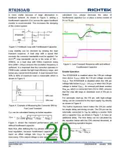
Place the FB resistors within 5mm of the FB pin.
Choose RFB2 between 10k and 100k to minimize
power consumption without excessive noise pick-up
and calculate RFB1 as follows :
RFB2 (VOUT VREF
VREF
)
RFB1
For output voltage accuracy, use divider resistors with
1% or better tolerance.
Feed-forward Capacitor Selection (CFF)
The RT6263A/B is optimized for low duty-cycle
applications and the control loop is stable with low ESR
ceramic output capacitors. In higher duty-cycle
applications (higher output voltages or lower input
voltages), the internal ripple signal will increase in
amplitude. Before the ACOT® control loop can react to
an output voltage fluctuation, the voltage change on the
feedback signal must exceed the internal ripple
amplitude. Because of the large internal ripple in this
condition, the response may become slower and
under-damped. This situation will result in ringing
waveform at output terminal. In case of high output
voltage application, the phenomenon described above
is a registered trademark of Richtek Technology Corporation.
VOUT
V fSW
IN
tON
tON
=
and DMAX =
tON tOFF_MIN
The real on-time will slightly extend due to the voltage
drop which is related to output current; however, this
on-time compensation can be neglected. Calculate the
output voltage sag as :
2
L(IOUT
)
VSAG
=
2COUT VIN(MIN) DMAX VOUT
The amplitude of the capacitive soar is a function of the
load step, the output capacitor value, the inductor value
and the output voltage :
Copyright © 2020 Richtek Technology Corporation. All rights reserved.
DS6263A/B-00 January 2020
www.richtek.com
19

 RICHTEK [ RICHTEK TECHNOLOGY CORPORATION ]