RT6263A/B
be lower than 5.5V.
5V
5V
D
BOOT
R
BOOT
BOOT
RT6263A/B
SW
D
BOOT
C
0.1μF
BOOT
BOOT
RT6263A/B
SW
C
0.1μF
BOOT
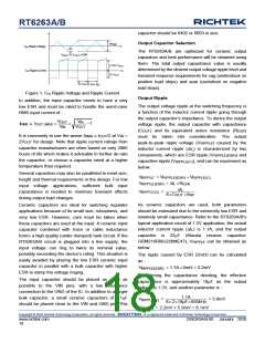
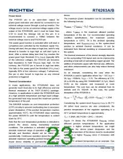
Figure 12. External Bootstrap Diode and Resistor at
the BOOT Pin
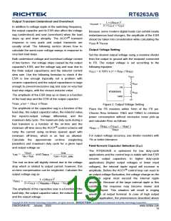
Figure 10. External Bootstrap Diode
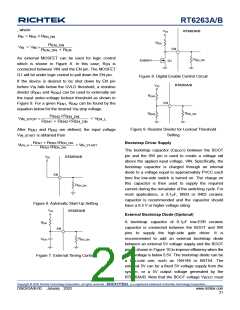
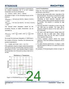
Soft-Start
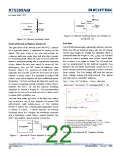
External Bootstrap Resistor (Optional)
The RT6263A/B provides adjustable soft-start function.
When the EN pin becomes logic-high, the SS charge
current (ISS) begins to charge the capacitor which is
connected from the SS pin to GND (CSS).The soft-start
function is used to prevent large inrush current while
the converter is in power-up stage The soft-start time
can be programmed by the external capacitor CSS
between SS and GND. An internal current source ISS
(6A) charges an external capacitor to build a soft-start
ramp voltage. The VFB voltage will track the internal
ramp voltage during soft-start interval. The typical
soft-start time is calculated as below :
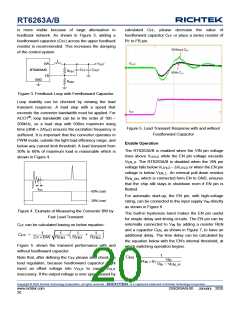
The gate driver of an internal power MOSFET, utilized
as a high-side switch, is optimized for turning on the
switch. The gate driver is not only fast enough for
reducing switching power loss, but also slow enough
for minimizing EMI. The EMI issue is worse when the
switch is turned on rapidly due to the induced high di/dt
noises. When the high-side switch is turned off, the
discharging time on SW node is relatively slow
because there’s the presence of dead time, both
high-side and low-side MOSFETs are turned off in this
interval. In some cases, it is desirable to reduce EMI
further, even at the expense of some additional power
dissipation. The turn-on rate of the high-side switch can
be slowed by placing a small bootstrap resistor RBOOT
between the BOOT pin and the external bootstrap
capacitor as shown in Figure 11. The recommended
range for the RBOOT is several ohms to 47 ohms, and it
could be 0402 or 0603 in size.
tSS = CSS 0.7V/30μA + CSS VFB/ISS
, where tSS = SS rises to FB settled point (T2 + T3)
EN
SS
SS = 1.9V
This will slow down the rates of the high-side switch
turn on and the rise of VSW. In order to improve EMI
performance and enhancement of the internal
MOSFET switch, the recommended application circuit
is shown in Figure 12, which includes an external
bootstrap diode for charging the bootstrap capacitor
and a bootstrap resistor RBOOT placed between the
BOOT pin and the capacitor/diode connection.
V1
FB
T1
T2
T3
PG
T1 : EN delay, from EN go high to SS start rising, T1 = 50μs;
T2 : speed up SS, from SS rising to FB start rising, T2 = C x 0.7/30μA;
R
BOOT
SS
BOOT
RT6263A/B
T3 : normal SS, from FB rising to settled, T3 = C x V /I
;
SS
V1 : offset voltage between SS and FB, V1 = 700mV;
PG go high after SSOK (SS = 1.9V)
FB SS
C
0.1μF
BOOT
SW
Figure 13. Operation of SS Pin when Starting
Figure 11. External Bootstrap Resistor at the BOOT
Pin
Copyright © 2020 Richtek Technology Corporation. All rights reserved.
is a registered trademark of Richtek Technology Corporation.
www.richtek.com
22
DS6263A/B-00 January 2020

 RICHTEK [ RICHTEK TECHNOLOGY CORPORATION ]