RT6263A/B
device.
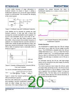
Power Good
The maximum power dissipation can be calculated by
the following formula :
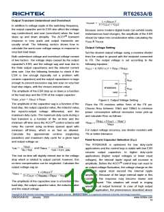
The PGOOD pin is an open-drain output for
power-good indication and should be connected to an
external voltage source through a pull-up resistor. The
voltage source can be an external voltage supply or the
output of the RT6263A/B, and it must be lower than
5.5V to avoid the damage risk on this pin. It is
recommended to connect a 100k between the
external voltage source and PGOOD pin.
PD MAX = T
TA / θ
J MAX
JA EFFECTIVE
, where TJ(MAX) is the maximum allowed junction
temperature of the die. For recommended operating
condition specifications, the maximum junction
temperature is 125°C. TA is the ambient operating
temperature, and θJA(EFFECTIVE) is the system-level
junction to ambient thermal resistance. It can be
estimated from thermal modeling or measurements in
the system.
The power-good function is activated after soft-start is
completed and controlled by the feedback signal VFB
.
During soft-start, this pin stays in logic-low, and it's only
allowed to transfer to logic-high as soft-start cycle is
done. After a certain delay time that VFB reaches the
power-good high threshold (VTH_PGLH) (typically 90%
of the reference voltage), the PGOOD pin becomes
high impedance to hold VPGOOD logic high. On the
contrary, the PGOOD pin is forced to logic-low while
The thermal resistance of the device strongly depends
on the surrounding PCB layout and can be improved by
providing a heat sink of surrounding copper ground. The
addition of backside copper with thermal vias, stiffeners,
and other enhancements can also help reduce thermal
resistance.
VFB falls to the power-good low threshold (VTH_PGHL
)
(typically 85% of the reference voltage). Furthermore,
this pin is also forced to logic-low as any internal
protection is triggered.
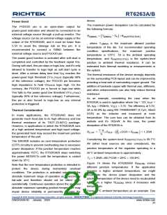
As an example, considering the case when the
RT6263A is used in application where VIN = 12V, IOUT
=
3A, fSW = 650kHz, VOUT = 3.3V. The efficiency at 3.3V,
3A is 85.9% by using WE-74404054047 (4.7H, 30m
DCR) as the inductor and measured at room
temperature. The core loss can be obtained from its
website and it’s 102mW. In this case, the power
dissipation of the RT6263A is
Thermal Consideration
In many applications, the RT6263A/B does not
generate much heat due to its high efficiency and low
thermal resistance of its TSOT-23-8(FC) package.
However, in applications in which the RT6263A/B runs
at a high ambient temperature and high input voltage,
the generated heat may exceed the maximum junction
temperature of the part.
1η
η
2
P
D, RT
=
P
I DCR + P
= 1.25W
OUT
CORE
O
Considering the system-level θJA(EFFECTIVE) is 68.7°C
/W (other heat sources are also considered), the
junction temperature of the regulator operating in a
25°C ambient temperature is approximately :
The 6263A/B includes an over-temperature protection
(OTP) circuitry to prevent overheating due to excessive
power dissipation. If the junction temperature reaches
approximately 155°C, the RT6263A/B stops switching
the power MOSFETs until the temperature is cooled
down by 35°C.
TJ = 1.25W68.7C/W + 25C = 110.9C
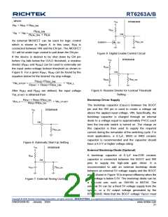
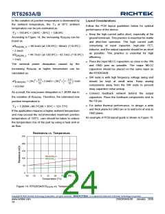
Figure 14 shows the RT6263A/B RDS(ON) versus
different junction temperatures. If the application
requires a higher ambient temperature, we might
recalculate the device power dissipation and the
junction temperature of the device need to recalculated
based on a higher RDS(ON) since it increases with
temperature.
Note that the over temperature protection is intended to
protect the device during momentary overload
conditions. The protection is activated outside of the
absolute maximum range of operation as a secondary
fail-safe and therefore should not be relied upon
operationally. Continuous operation above the specified
absolute maximum operating junction temperature may
impair device reliability or permanently damage the
Using 35°C ambient temperature as an example. Due
Copyright © 2020 Richtek Technology Corporation. All rights reserved.
is a registered trademark of Richtek Technology Corporation.
DS6263A/B-00 January 2020
www.richtek.com
23

 RICHTEK [ RICHTEK TECHNOLOGY CORPORATION ]