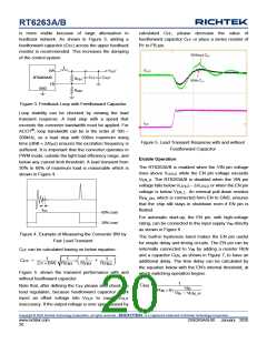
RT6263A/B
is more visible because of large attenuation in
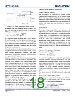
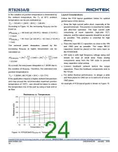
feedback network. As shown in Figure 3, adding a
feedforward capacitor (CFF) across the upper feedback
resistor is recommended. This increases the damping
of the control system.
calculated CFF, please decrease the value of
feedforward capacitor CFF or place a series resistor of
RT to FB pin.
L
SW
RT6263A/B
FB
V
OUT
C
OUT
C
FF
R
R
FB1
GND
FB2
Figure 3. Feedback Loop with Feedforward Capacitor
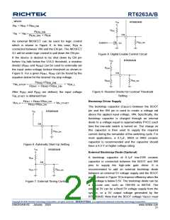
Loop stability can be checked by viewing the load
transient response. A load step with a speed that
exceeds the converter bandwidth must be applied. For
ACOT® , loop bandwidth can be in the order of 100 ~
200kHz, so a load step with 500ns maximum rising
time (dI/dt 2A/s) ensures the excitation frequency is
sufficient. It is important that the converter operates in
PWM mode, outside the light load efficiency range, and
below any current limit threshold. A load transient from
30% to 60% of maximum load is reasonable which is
shown in Figure 4.
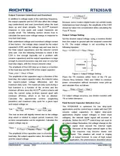
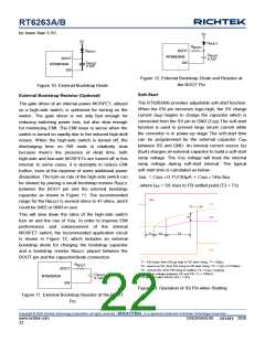
Figure 5. Load Transient Response with and without
Feedforward Capacitor
Enable Operation
The RT6263A/B is enabled when the VIN pin voltage
rises above VUVLO while the EN pin voltage exceeds
VEN_H. The RT6263A/B is disabled when the VIN pin
voltage falls below VUVLO VUVLO or when the EN pin
voltage is below VEN_L. An internal pull-down resistor
REN_DN, which is connected form EN to GND, ensures
that the chip still stays in shutdown even if EN pin is
floated.
f
CO
60% Load
30% Load
For automatic start-up, the EN pin, with high-voltage
rating, can be connected to the input supply VIN directly
as shown in Figure 6.
Figure 4. Example of Measuring the Converter BW by
Fast Load Transient
The built-in hysteresis band makes the EN pin useful
for simple delay and timing circuits. The EN pin can be
externally connected to VIN by adding a resistor REN
and a capacitor CEN, as shown in Figure 7, to have an
additional delay. The time delay can be calculated by
the equation below with the EN's internal threshold, at
which switching operation begins.
CFF can be calculated basing on below equation :
1
1
FB1
1
FB1
1
FB2
C
FF
=
+
2 BW R
R
R
Figure 5. shows the transient performance with and
without feedfoward capacitor.
t
C
EN
=
Note that, after defining the CFF please also check the
load regulation, because feedforward capacitor might
inject an offset voltage into VOUT to cause VOUT
inaccuracy. If the output voltage is over spec caused by
V
th
R ln
th
V V
th
EN_H
Copyright © 2020 Richtek Technology Corporation. All rights reserved.
is a registered trademark of Richtek Technology Corporation.
www.richtek.com
20
DS6263A/B-00 January 2020

 RICHTEK [ RICHTEK TECHNOLOGY CORPORATION ]