RX62Nグループ、RX621グループ
5. Electrical Characteristics
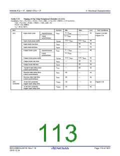
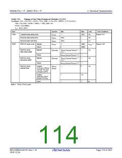
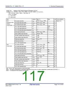
Table 5.16
Timing of On-Chip Peripheral Modules (4) (1/2)
Conditions: VCC = PLLVCC = AVCC = VCC_USB = 2.7 to 3.6V, VREFH = 2.7V to AVCC
VSS = PLLVSS = AVSS = VREFL = VSS_USB = 0V
PCLK = 8 to 50MHz
Ta = -40 to +85C
Ta = -40 to +85C
Min.*1*2
Item
Symbol
tSCL
tSCLH
tSCLL
tSr
Max.
Unit Test Conditions
6(12) × tIICcyc + 1300
—
RIIC
SCL input cycle time
ns Figure 5.43
(Standard-mode,
SMBus)
3(6) × tIICcyc + 300
—
SCL input high pulse width
SCL input low pulse width
SCL, SDA input rising time
SCL, SDA input falling time
ns
ns
ns
ns
ns
ns
ns
ns
ns
ns
ns
pF
ns
ns
ns
ns
ns
ns
ns
ns
ns
ns
ns
ns
pF
3(6) × tIICcyc + 300
—
ICFER.FMPE = 0
—
1000
—
300
tSf
0
1(4) × tIICcy
SCL, SDA input spike pulse removal time tSP
3(6) × tIICcyc + 300
—
SDA input bus free time
Start condition input hold time
Re-start condition input setup time
Stop condition input setup time
Data input setup time
tBUF
tIICcyc + 300
—
tSTAH
tSTAS
tSTOS
tSDAS
tSDAH
Cb
1000
—
1000
—
tIICcyc + 50
—
0
—
Data input hold time
—
400
SCL, SDA capacitive load
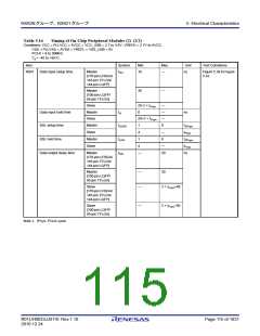
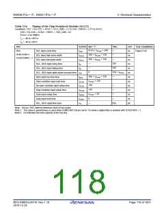
SCL input cycle time
6(12) × tIICcy + 600
3(6) × tIICcy + 300
3(6) × tIICcy + 300
20+0.1Cb
20+0.1Cb
0
—
RIIC
tSCL
tSCLH
tSCLL
tSr
(Fast-mode)
—
SCL input high pulse width
SCL input low pulse width
SCL, SDA input rising time
SCL, SDA input falling time
—
300
300
tSf
1(4) × tIICcy
SCL, SDA input spike pulse removal time tSP
3(6) × tIICcy + 300
tIICcy + 300
300
—
—
—
—
—
—
SDA input bus free time
tBUF
Start condition input hold time
Re-start condition input setup time
Stop condition input setup time
Data input setup time
tSTAH
tSTAS
tSTOS
tSDAS
tSDAH
Cb
300
tIICcy + 50
0
Data input hold time
SCL, SDA capacitive load
—
400
Note: tIICcyc: RIIC internal reference clock (IICφ) cycles
Note 1. The value in parentheses is used when ICMR3.NF[1:0] are set to 11b while a digital filter is enabled with ICFER.NFE = 1.
Note 2. Cb indicates the total capacity of the bus line.
R01UH0033JJ0110 Rev.1.10
2010.12.24
Page 117 of 1931

 RENESAS [ RENESAS TECHNOLOGY CORP ]