RX62Nグループ、RX621グループ
5. Electrical Characteristics
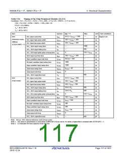
Table 5.18
Timing of On-Chip Peripheral Modules (6)
Conditions: VCC = PLLVCC = AVCC = VCC_USB = 2.7 to 3.6V, VREFH = 2.7V to AVCC
VSS = PLLVSS = AVSS = VREFL = VSS_USB = 0V
PCLK = 8 to 50MHz
Ta = -40 to +85C
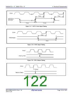
Item
Symbol
tTCKcyc
Min.
100
Typ.
—
Max.
—
Unit
Test Conditions
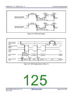
Figure 5.58
TCK clock cycle time
ns
TCK clock high pulse width
TCK clock low pulse width
TCK clock rising time
TCK clock falling time
TRST# pulse width
TMS setup time
tTCKH
tTCKL
tTCKr
45
45
—
—
20
20
20
20
20
—
—
—
—
—
—
—
—
—
—
—
—
—
5
ns
ns
ns
tTCKf
5
ns
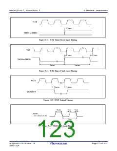
tTRSTW
tTMSS
tTMSH
tTDIS
—
—
—
—
—
40
tTCKcyc
ns
Figure 5.59
Figure 5.60
TMS hold time
ns
TDI setup time
ns
TDI hold time
tTDIH
ns
TDO data delay time
tTDOD
ns
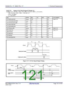
T1
T2
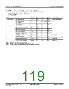
PCLK
tPRS tPRH
Input port (read)
tPWD
Output port (write)
Figure 5.25 I/O Port Input/Output Timing
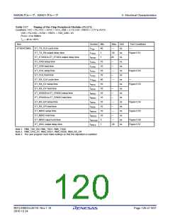
PCLK
tTOCD
Output
compare output
tTICS
Input capture
input
tTICW
Figure 5.26 MTU2 Input/Output Timing
R01UH0033JJ0110 Rev.1.10
2010.12.24
Page 121 of 1931

 RENESAS [ RENESAS TECHNOLOGY CORP ]